20-pin J-Link Connector
This article describes the 20-pin J-Link Connector, available on all J-Links (except for EDU mini), J-Trace & Flasher models.
Contents
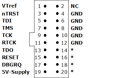
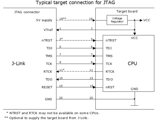
Pinout for JTAG
J-Link and J-Trace have a JTAG connector compatible to ARM's Multi-ICE. The JTAG connector is a 20 way Insulation Displacement Connector (IDC) keyed box header (2.54mm male) that mates with IDC sockets mounted on a ribbon cable.
(*) On some models like the J-Link ULTRA, these pins are reserved for firmware extension purposes.
They can be left open or connected to GND in normal debug environment.
Please do not assume them to be connected to GND inside J-Link.
The following table lists the J-Link / J-Trace JTAG pinout.
| PIN | SIGNAL | TYPE | Description |
|---|---|---|---|
| 1 | VTref | Input | This is the target reference voltage. It is used to check if the target has power, to create the logic-level reference for the input comparators and to control the output logic levels to the target. It is normally fed from VDD of the target board and must not have a series resistor. |
| 2 | Not connected | NC | This pin is not connected. |
| 3 | nTRST | Output | JTAG Reset. Output from J-Link to the Reset signal of the target JTAG port. Typically connected to nTRST of the target CPU. This pin is normally pulled HIGH on the target to avoid unintentional resets when there is no connection. |
| 5 | TDI | Output | JTAG data input of target CPU. It is recommended that this pin is pulled to a defined state on the target board. Typically connected to TDI of the target CPU. |
| 7 | TMS | Output | JTAG mode set input of target CPU. This pin should be pulled up on the target. Typically connected to TMS of the target CPU. |
| 9 | TCK | Output | JTAG clock signal to target CPU. It is recommended that this pin is pulled to a defined state of the target board. Typically connected to TCK of the target CPU. |
| 11 | RTCK | Input | Return test clock signal from the target. Some targets must synchronize the JTAG inputs to internal clocks. To assist in meeting this requirement, you can use a returned, and adjusted, TCK to dynamically control the TCK rate. J-Link supports adaptive clocking, which waits for TCK changes to be echoed correctly before making further changes. Connect to RTCK if available, otherwise to GND. |
| 13 | TDO | Input | JTAG data output from target CPU. Typically connected to TDO of the target CPU. |
| 15 | nRESET | I/O | Target CPU reset signal. Typically connected to the RESET pin of the target CPU, which is typically called "nRST", "nRESET" or "RESET". This signal is an active low signal. |
| 17 | DBGRQ | NC | This pin is not connected in J-Link. It is reserved for compatibility with other equipment to be used as a debug request signal to the target system. Typically connected to DBGRQ if available, otherwise left open. |
| 19 | 5V-Supply | Output | This pin can be used to supply power to the target hardware. Older J-Links may not be able to supply power on this pin. For more information about how to enable/disable the power supply, please refer to Target power supply. |
| 4, 6, 8, 10, 12 | GND | Ground | GND pins connected to GND in J-Link. They should also be connected to GND in the target system. |
| 14, 16, 18, 20 | Res | Reserved | On some models like the J-Link ULTRA, these pins are reserved for firmware extension purposes. They can be left open or connected to GND in normal debug environment. They are not essential for JTAG or SWD in general Please do not assume them to be connected to GND inside J-Link. |
Target board design
We strongly advise following the recommendations given by the chip manufacturer.
These recommendations are normally in line with the recommendations given in the table Pinout for JTAG.
In case of doubt you should follow the recommendations given by the semiconductor manufacturer.
You may take any female header following the specifications of DIN 41651.
For example:
| Harting | part-no. 09185206803 |
| Molex | part-no. 90635-1202 |
| Tyco Electronics | part-no. 2-215882-0 |
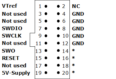
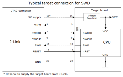
Pinout for SWD
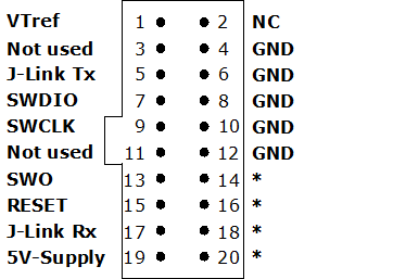
The J-Link and J-Trace JTAG connector is also compatible to ARM's Serial Wire Debug (SWD).
(*) On some models like the J-Link ULTRA, these pins are reserved for firmware extension purposes.
They can be left open or connected to GND in normal debug environment.
Please do not assume them to be connected to GND inside J-Link.
The following table lists the J-Link / J-Trace SWD pinout.
| PIN | SIGNAL | TYPE | Description |
|---|---|---|---|
| 1 | VTref | Input | This is the target reference voltage. It is used to check if the target has power, to create the logic-level reference for the input comparators and to control the output logic levels to the target. It is normally fed from VDD of the target board and must not have a series resistor. |
| 2 | Not connected | NC | This pin is not connected. |
| 3 | Not used | NC | This pin is not used by J-Link when selecting SWD as interface type. If the device may also be accessed via JTAG, this pin may be connected to nTRST, otherwise leave open. |
| 5 | Not used | NC | This pin is not used by J-Link when selecting SWD as interface type. If the device may also be accessed via JTAG, this pin may be connected to TDI, otherwise leave open. |
| 7 | SWDIO | Output | JTAG mode set input of target CPU. This pin should be pulled up on the target. Typically connected to TMS of the target CPU. |
| 9 | SWCLK | Output | JTAG clock signal to target CPU. It is recommended that this pin is pulled to a defined state of the target board. Typically connected to TCK of the target CPU. |
| 11 | Not used | NC | This pin is not used by J-Link when selecting SWD as interface type. If the device may also be accessed via JTAG, this pin may be connected to RTCK, otherwise leave open. |
| 13 | SWO | Input | Serial Wire Output trace port. (Optional, not required for SWD communication.) |
| 15 | nRESET | I/O | Target CPU reset signal. Typically connected to the RESET pin of the target CPU, which is typically called "nRST", "nRESET" or "RESET". This signal is an active low signal. |
| 17 | Not used | NC | This pin is not connected in J-Link. |
| 19 | 5V-Supply | Output | This pin can be used to supply power to the target hardware. Older J-Links may not be able to supply power on this pin. For more information about how to enable/disable the power supply, please refer to Target power supply. |
| 4, 6, 8, 10, 12 | GND | Ground | GND pins connected to GND in J-Link. They should also be connected to GND in the target system. |
| 14, 16, 18, 20 | Res | Reserved | On some models like the J-Link ULTRA, these pins are reserved for firmware extension purposes. They can be left open or connected to GND in normal debug environment. They are not essential for JTAG or SWD in general Please do not assume them to be connected to GND inside J-Link. |
Target board design
We strongly advise following the recommendations given by the chip manufacturer.
These recommendations are normally in line with the recommendations given in the table Pinout for SWD.
In case of doubt you should follow the recommendations given by the semiconductor manufacturer.
Pinout for SWD + Virtual COM Port (VCOM)
The J-Link and J-Trace JTAG connector is also compatible to ARM's Serial Wire Debug (SWD).
(*) On some models like the J-Link ULTRA, these pins are reserved for firmware extension purposes.
They can be left open or connected to GND in normal debug environment.
Please do not assume them to be connected to GND inside J-Link.
The following table lists the J-Link / J-Trace SWD pinout.
| PIN | SIGNAL | TYPE | Description |
|---|---|---|---|
| 1 | VTref | Input | This is the target reference voltage. It is used to check if the target has power, to create the logic-level reference for the input comparators and to control the output logic levels to the target. It is normally fed from VDD of the target board and must not have a series resistor. |
| 2 | Not connected | NC | This pin is not connected. |
| 3 | Not used | NC | This pin is not used by J-Link when selecting SWD as interface type. If the device may also be accessed via JTAG, this pin may be connected to nTRST, otherwise leave open. |
| 5 | J-Link Tx | Output | This pin is used as VCOM Tx (out on J-Link side) in case VCOM functionality of J-Link is enabled. For further information about VCOM, please refer to VCOM |
| 7 | SWDIO | Output | JTAG mode set input of target CPU. This pin should be pulled up on the target. Typically connected to TMS of the target CPU. |
| 9 | SWCLK | Output | JTAG clock signal to target CPU. It is recommended that this pin is pulled to a defined state of the target board. Typically connected to TCK of the target CPU. |
| 11 | Not used | NC | This pin is not used by J-Link when selecting SWD as interface type. If the device may also be accessed via JTAG, this pin may be connected to RTCK, otherwise leave open. |
| 13 | SWO | Input | Serial Wire Output trace port. (Optional, not required for SWD communication.) |
| 15 | nRESET | I/O | Target CPU reset signal. Typically connected to the RESET pin of the target CPU, which is typically called "nRST", "nRESET" or "RESET". This signal is an active low signal. |
| 17 | J-Link Rx | Input | This pin is used as VCOM Rx (in on J-Link side) in case VCOM functionality of J-Link is enabled. For further information, please refer to VCOM. |
| 19 | 5V-Supply | Output | This pin can be used to supply power to the target hardware. Older J-Links may not be able to supply power on this pin. For more information about how to enable/disable the power supply, please refer to Target power supply. |
| 4, 6, 8, 10, 12 | GND | Ground | GND pins connected to GND in J-Link. They should also be connected to GND in the target system. |
| 14, 16, 18, 20 | Res | Reserved | On some models like the J-Link ULTRA, these pins are reserved for firmware extension purposes. They can be left open or connected to GND in normal debug environment. They are not essential for JTAG or SWD in general Please do not assume them to be connected to GND inside J-Link. |
Pinout for SPI
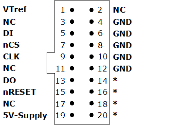
(*) On some models like the J-Link ULTRA, these pins are reserved for firmware extension purposes.
They can be left open or connected to GND in normal debug environment.
Please do not assume them to be connected to GND inside J-Link.
The following table lists the pinout for the SPI interface on J-Link.
| PIN | SIGNAL | TYPE | Description |
|---|---|---|---|
| 1 | VTref | Input | This is the target reference voltage. It is used to check if the target has power, to create the logic-level reference for the input comparators and to control the output logic levels to the target. It is normally fed from VDD of the target board and must not have a series resistor. |
| 2 | Not connected | NC | This pin is not connected. Leave open on target side |
| 3 | Not connected | NC | This pin is not connected. Leave open on target side |
| 5 | DI | Output | Data-input of target SPI. Output of J-Link, used to transmit data to the target SPI. |
| 7 | nCS | Output | Chip-select of target SPI (active LOW). |
| 9 | CLK | Output | SPI clock signal. |
| 11 | Not connected | NC | This pin is not connected. Leave open on target side |
| 13 | DO | Input | Data-out of target SPI. Input of J-Link, used to receive data from the target SPI. |
| 15 | nRESET | I/O | Target CPU reset signal. |
| 17 | Not connected | NC | This pin is not connected. Leave open on target side |
| 19 | 5V-Supply | Output | This pin can be used to supply power to the target hardware. Older J-Links may not be able to supply power on this pin. For more information about how to enable/disable the power supply, please refer to Target power supply. |
| 4, 6, 8, 10, 12 | GND | Ground | GND pins connected to GND in J-Link. They should also be connected to GND in the target system. |
| 14, 16, 18, 20 | Res | Reserved | On some models like the J-Link ULTRA, these pins are reserved for firmware extension purposes. They can be left open or connected to GND in normal debug environment. They are not essential for JTAG or SWD in general Please do not assume them to be connected to GND inside J-Link. |
Pinout for QSPI
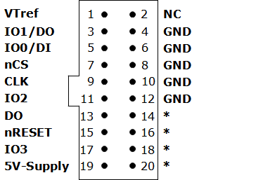
(*) On some models like the J-Link ULTRA, these pins are reserved for firmware extension purposes.
They can be left open or connected to GND in normal debug environment.
Please do not assume them to be connected to GND inside J-Link.
The following table lists the pinout for the QSPI interface on J-Link.
| PIN | SIGNAL | TYPE | Description |
|---|---|---|---|
| 1 | VTref | Input | This is the target reference voltage It is used to check if the target has power, to create the logic-level reference for the input comparators and to control the output logic levels to the target. It is normally fed from Vdd of the target board and must not have a series resistor. |
| 2 | Not\n connected | NC | Leave open on target side |
| 3 | IO1 | I/O | Bi-directional data I/O pin 1 |
| 5 | IO0/DI | I/O | Single: Data-input of target SPI. Output of programmer, used to transmit data to the target SPI. Quad: Bi-directional data I/O pin 0 |
| 7 | nCS | Output | Chip-select of target SPI (active LOW). |
| 9 | CLK | Output | SPI clock signal. |
| 11 | IO2 | I/O | Bi-directional data I/O pin 2 |
| 13 | DO | Input | Single: Data-out of target SPI. Input of programmer, used to receive data from the target SPI. Quad: Must be connected to same signal as pin 3 IO1/DO to guarantee correct operation for temporary single mode transfers during QSPI mode. |
| 15 | nRESET | Output | Target CPU reset signal (active LOW). Typically connected to the reset pin of the target CPU, which is typically called "nRST", "nRESET" or "RESET". |
| 17 | IO3 | I/O | Bi-directional data I/O pin 3 |
| 19 | 5V-Supply | Output | This pin can be used to supply power to the target hardware. Older J-Links may not be able to supply power on this pin. |
| 4, 6, 8, 10, 12 | GND | Ground | GND pins connected to GND in J-Link. They should also be connected to GND in the target system. |
| 14, 16, 18, 20 | Res | Reserved | On some models like the J-Link ULTRA, these pins are reserved for firmware extension purposes. They can be left open or connected to GND in normal debug environment. They are not essential for JTAG or SWD in general Please do not assume them to be connected to GND inside J-Link. |
Adapters
There are many J-Link Adapters available to be used with the J-Link 20-pin connector. Please refer to the SEGGER Homepage for a list of available adapters.
