GigaDevice GD32E231C-START
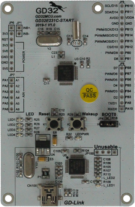
This article describes specifics for the GigaDevice GD32E231C-START evaluation board.
Minimum requirements
- J-Link software V6.87b or later
Preparing for J-Link
!! NOTE: The following guide, if done incorrectly, might damage your board !!
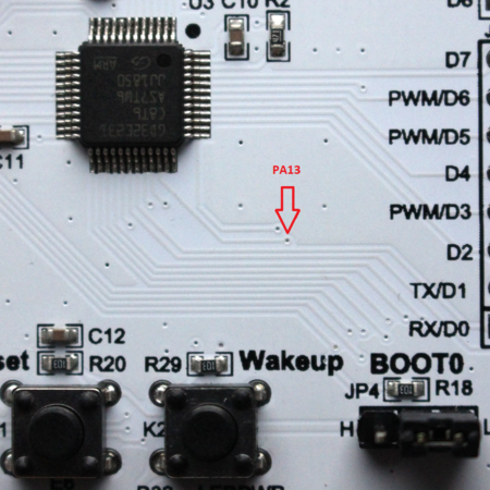
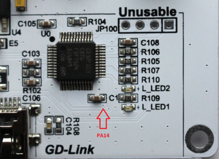
The GD32E231C-START does not have the SWDIO and SWCLK lines accessible via pins. The only way to get access to the SWDIO and CLK lines, is to scratch the board open on the correct positions as shown in the images below. Be sure that you are scratching at the right position, otherwise your board might be damaged beyond recovery. Then you can connect the line by soldering a jumping wire to it.
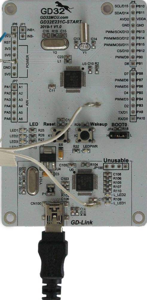
After that, connect the board with the soldered on jumping wires to your J-Link (see table below)
For information about the J-Link pinout please refer to the following page: J-Link SWD pinout.
| J-Link 20 pin debug interface | Pin on evaluation board |
|---|---|
| Pin 1 (VTref) | +3V3 |
| Pin 4 (GND) | GND |
| Pin 7 (SWDIO) | PA13 |
| Pin 9 (SWCLK) | PA14 |
The result should be looking like this:
- Power the board via the USB port (CN100).
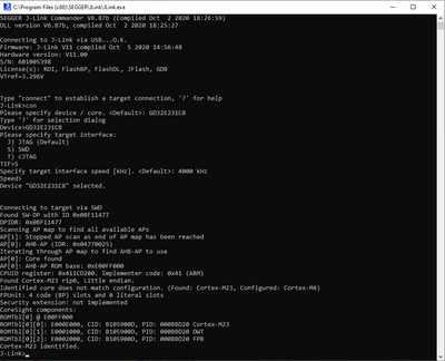
- Verify the Connection with e.g. J-Link Commander. The output should look as follows:
Example Project
The following example project was created with the SEGGER Embedded Studio project wizard and runs out-of-the-box on the GigaDevice GD32E231C-START. It is a simple blinky application which toggles LED1. The application is linked into the internal flash.
SETUP
- J-Link software: V6.87b
- Embedded Studio: V4.52b (or later)
- Hardware: GigaDevice GD32E231C-START
- Link: File:GigaDevice GD32E231C TestProject ES V452b.zip
