Target Interface JTAG
JTAG is the acronym for Joint Test Action Group. In the scope of this document, "the JTAG standard" means compliance with IEEE Standard 1149.1-2001. Initially designed to verify designs and PCBs after manufacturing them, it has developed and extended over time and finally also become a standard to define debug interfaces for CPUs.
Contents
Test access port (TAP)
JTAG defines a TAP (Test access port). The TAP is a general-purpose port that can provide access to many test support functions built into a component. It is composed as a minimum of the three input connections (TDI, TCK, TMS) and one output connection (TDO). An optional fourth input connection (nTRST) provides for asynchronous initialization of the test logic.
| Pin | Type | Explanation |
|---|---|---|
| TCK | Input | The test clock input (TCK) provides the clock for the test logic. |
| TDI | Input | Serial test instructions and data are received by the test logic at test data input (TDI). |
| TMS | Input | The signal received at test mode select (TMS) is decoded by the TAP controller to control test operations. |
| TDO | Output | Test data output (TDO) is the serial output for test instructions and data from the test logic. |
| nTRST | Input (optional) | The optional test reset (nTRST) input provides for asynchronous initialization of the TAP controller. |
The TAP controller
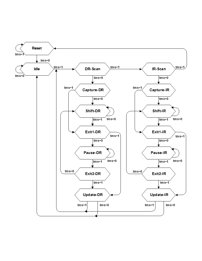
The TAP controller is a synchronous finite state machine that responds to changes at the TMS and TCK signals of the TAP and controls the sequence of operations of the circuitry. TAP controller state diagram
Data registers (DR-Scan path)
JTAG requires at least two data registers to be present: the bypass and the boundary-scan register. Other registers are allowed but are not obligatory.
Bypass data register
A single-bit register that passes information from TDI to TDO.
Boundary-scan data register
A test data register which allows the testing of board interconnections, access to input and output of components when testing their system logic and so on.
Instruction register (IR-Scan path)
The instruction register holds the current instruction and its content is used by the TAP controller to decide which test to perform or which data register to access. It consist of at least two shift-register cells.
State descriptions
Reset
The test logic is disabled so that normal operation of the chip logic can continue unhindered. No matter in which state the TAP controller currently is, it can change into Reset state if TMS is high for at least 5 clock cycles. As long as TMS is high, the TAP controller remains in Reset state.
Idle
Idle is a TAP controller state between scan (DR or IR) operations. Once entered, this state remains active as long as TMS is low.
DR-Scan
Temporary controller state. If TMS remains low, a scan sequence for the selected data registers is initiated.
IR-Scan
Temporary controller state. If TMS remains low, a scan sequence for the instruction register is initiated.
Capture-DR
Data may be loaded in parallel to the selected test data registers.
Shift-DR
The test data register connected between TDI and TDO shifts data one stage towards the serial output with each clock.
Exit1-DR
Temporary controller state.
Pause-DR
The shifting of the test data register between TDI and TDO is temporarily halted.
Exit2-DR
Temporary controller state. Allows to either go back into Shift-DR state or go on to Update-DR.
Update-DR
Data contained in the currently selected data register is loaded into a latched parallel output (for registers that have such a latch). The parallel latch prevents changes at the parallel output of these registers from occurring during the shifting process.
Capture-IR
Instructions may be loaded in parallel into the instruction register.
Shift-IR
The instruction register shifts the values in the instruction register towards TDO with each clock.
Exit1-IR
Temporary controller state.
Pause-IR
Wait state that temporarily halts the instruction shifting.
Exit2-IR
Temporary controller state. Allows to either go back into Shift-IR state or go on to Update-IR.
Update-IR
The values contained in the instruction register are loaded into a latched parallel out- put from the shift-register path. Once latched, this new instruction becomes the cur- rent one. The parallel latch prevents changes at the parallel output of the instruction register from occurring during the shifting process.
