ST STM32F4
This article describes device specifics of the ST STM32F4 series devices. The STM32F4 devices are Cortex-M0 based MCUs with low-power functionality.
Contents
Flash Banks
Internal Flash
The following flash regions are supported by J-Link.
| Device | Base address | Size | J-Link Support |
|---|---|---|---|
| STM32F4xxx8 | 0x08000000 | 64 KB | |
| STM32F4xxxB | 0x08000000 | 128 KB | |
| STM32F4xxxC | 0x08000000 | 256 KB | |
| STM32F4xxxD | 0x08000000 | 384 KB | |
| STM32F4xxxE | 0x08000000 | 512 KB | |
| STM32F4xxxG | 0x08000000 | 1024 KB | |
| STM32F4xxxH | 0x08000000 | 1536 KB | |
| STM32F4xxxI | 0x08000000 | 2048 KB |
QSPI Flash
QSPI flash programming requires special handling compared to internal flash. For more information about this, please see the QSPI Flash Programming Support article.
Some ST STM32F4 device series come with a QUADSPI controller which allows memory mapped read accesses to any (Q)SPI flash, connected to the QUADSPI interface of the MCU.
J-Link supports for the STM32F446/STM32F469 devices:
- One single or quad SPI device connected to BK1
Two single or quad SPI devices are not supported yet (dual mode).
J-Link supports multiple pin configurations for STM32F4xx. The default loader is marked in bold.
| Device | Base address | Maximum size | Supported pin configuration |
|---|---|---|---|
| STM32F412 | 0x90000000 | up to 64 MB | CLK@PB2_nCS@PG6_D0@PF8_D1@PF9_D2@PF7_D3@PF6 |
| STM32F446 | 0x90000000 | up to 64 MB | CLK@PD3_nCS@PG6_D0@PF8_D1@PF9_D2@PF7_D3@PF6 |
| STM32F469 | 0x90000000 | up to 64 MB | CLK@PF10_nCS@PB6_D0@PF8_D1@PF9_D2@PF7_D3@PF6 |
For pin configuration, different from the one used in the example flash algorithm, please get in touch with SEGGER directly via our support system: https://www.segger.com/ticket/.
Reset
For the STM32F4 devices, the Cortex-M default reset strategy is used.
Debug specific
Please refer to the general STM32 article
Option byte programming
The STM32F4 series devices provide some option bytes which allow some "permanent" configuration as well as readout protection for the device. Unfortunately, the option bytes become effective immediately when programmed. This means when enabling the read protection of the device via option bytes, the programmer will immediately lose the access to the flash, without any possibility to verify the complete flash operation. Therefore, the option bytes cannot be programmed as part of the flash image. The sequence, to program the option bytes consists of multiple read / write accesses to special function registers of the STM32F4 MCU.
Via J-Flash / Flasher ARM
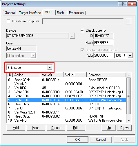
The sequence to program the option bytes, needs to be added to the exit-steps of the J-Flash project. The exit steps will be executed at the end of an successful auto-programming process (Target -> Auto). J-Flash comes with an example project for the STM32F405OE which contains the option byte programming sequence (File:STM32F405OE OptBytes.jflash). This sequence applies for all STM32F2 / F4 devices since they are compatible regarding option byte programming and can be adapted to fit custom requirements. The option byte values are transmitted in exit step # 5, which writes the OPTCR.

Modification example (seting WDG_SW byte and read protection bit)
As mentioned above, the option bytes can be customized by changing step # 5 of the Exit steps above.
Necessary changes of "Step 5" in "Data" section:
| Value | Effect |
|---|---|
| 0x0FFFAABC | Read protection level 0, WDG_SW set to Hardware independent watchdog |
| 0x0FFFAAEC | Read protection level 0, WDG_SW set to Software independent watchdog |
| 0x0FFFBBBC | Read protection level 1, WDG_SW set to Hardware independent watchdog |
| 0x0FFFBBEC | Read protection level 1, WDG_SW set to Software independent watchdog |
| 0x0FFFCCBC | Read protection level 2, WDG_SW set to Hardware independent watchdog |
| 0x0FFFCCEC | Read protection level 2, WDG_SW set to Software independent watchdog |
- For STM32F42xxx and STM32F43xxx devices, bit 4 is used for setting the single or dual bank flash memory option. In this example the default case (single bank flash memory) was selected.
- After changing WDG_SW, the device must be reset for the changes to take effect.
Securing/unsecuring the device
Please refer to the generic wiki-article: STM32#MCU_Security
RTT
SEGGER's RTT can be used with a J-Link connected to a STM32F4 target device.
Sample project
For a sample Embedded Studio project, refer to the following .zip archive:
ST_STM32F446ZE_NUCLEO_RTT.zip
The above project was tested with the following setup:
| Target device | STM32F446ZE |
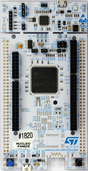
| Evalboard | NUCLEO-F446ZE (ST) |
| J-Link software version | V6.51b |
| Embedded Studio version | V4.18 |
