Difference between revisions of "NXP S32K3xx"
(→Limitations) |
(→Multi-Core Support) |
||
| (40 intermediate revisions by 3 users not shown) | |||
| Line 1: | Line 1: | ||
__TOC__ |
__TOC__ |
||
| − | The S32K3 family from NXP includes Cortex-M7 based MCUs in single or dual core configurations supporting ASIL B/D safety applications. The S32K3 family is supported since J-Link software version V6.89c. |
+ | The S32K3 family from NXP includes Cortex-M7 based MCUs in single or dual core configurations supporting ASIL B/D safety applications. The S32K3 family is supported since J-Link software version V6.89c. |
| − | '''NOTE:''' There are different device configurations available. For details regarding which configurations are available and which are supported by the J-Link software, please get in touch with NXP (NDA required). Due to the fact that most device information are under NDA, SEGGER is allowed to provide very limited support, only. If you encounter any issues with the S32K3 device support, we recommend to get in touch with NXP directly. They will involve us if required. |
||
| − | |||
==Internal Flash== |
==Internal Flash== |
||
===Supported Regions=== |
===Supported Regions=== |
||
| + | ====S32K311==== |
||
| − | Following flash regions are supported by the J-Link: |
||
| + | {| class="seggertable" |
||
| − | *Code flash memory 0 (0x00400000 - 0x004FFFFF) |
||
| + | |- |
||
| − | *Code flash memory 1 (0x00500000 - 0x005FFFFF) |
||
| + | ! Flash Bank || Base address !! Size || J-Link Support |
||
| − | *Code flash memory 2 (0x00600000 - 0x006FFFFF) |
||
| + | |- |
||
| − | *Code flash memory 3 (0x00700000 - 0x007F3FFF) |
||
| + | | Code flash 0 || 0x00400000 || Up to 512 KB || style="text-align:center;"| {{YES}} |
||
| − | *Data flash memory (0x10000000 - 0x1003FFFF) |
||
| + | |- |
||
| − | ==RAM== |
||
| + | | Code flash 1 || 0x00480000 || Up to 512 KB || style="text-align:center;"| {{YES}} |
||
| + | |- |
||
| + | | Data flash || 0x10000000 || Up to 64 KB || style="text-align:center;"| {{YES}} |
||
| + | |- |
||
| + | | UTEST || 0x1B000000 || Up to 8 KB || style="text-align:center;"| {{NO}} |
||
| + | |} |
||
| + | |||
| + | ====S32K312, S32K322 and S32K342==== |
||
| + | {| class="seggertable" |
||
| + | |- |
||
| + | ! Flash Bank || Base address !! Size || J-Link Support |
||
| + | |- |
||
| + | | Code flash 0 || 0x00400000 || Up to 1 MB || style="text-align:center;"| {{YES}} |
||
| + | |- |
||
| + | | Code flash 1 || 0x00500000 || Up to 1 MB || style="text-align:center;"| {{YES}} |
||
| + | |- |
||
| + | | Data flash || 0x10000000 || Up to 128 KB || style="text-align:center;"| {{YES}} |
||
| + | |- |
||
| + | | UTEST || 0x1B000000 || Up to 8 KB || style="text-align:center;"| {{NO}} |
||
| + | |} |
||
| + | |||
| + | ====S32K314, S32K324 and S32K344==== |
||
| + | {| class="seggertable" |
||
| + | |- |
||
| + | ! Flash Bank || Base address !! Size || J-Link Support |
||
| + | |- |
||
| + | | Code flash 0 || 0x00400000 || Up to 1 MB || style="text-align:center;"| {{YES}} |
||
| + | |- |
||
| + | | Code flash 1 || 0x00500000 || Up to 1 MB || style="text-align:center;"| {{YES}} |
||
| + | |- |
||
| + | | Code flash 2 || 0x00600000 || Up to 1 MB || style="text-align:center;"| {{YES}} |
||
| + | |- |
||
| + | | Code flash 3 || 0x00700000 || Up to 1 MB || style="text-align:center;"| {{YES}} |
||
| + | |- |
||
| + | | Data flash || 0x10000000 || Up to 128 KB || style="text-align:center;"| {{YES}} |
||
| + | |- |
||
| + | | UTEST || 0x1B000000 || Up to 8 KB || style="text-align:center;"| {{NO}} |
||
| + | |} |
||
| + | |||
| + | ====S32K358 and S32K388==== |
||
| + | {| class="seggertable" |
||
| + | |- |
||
| + | ! Flash Bank || Base address !! Size || J-Link Support |
||
| + | |- |
||
| + | | Code flash 0 || 0x00400000 || Up to 2 MB || style="text-align:center;"| {{YES}} |
||
| + | |- |
||
| + | | Code flash 1 || 0x00600000 || Up to 2 MB || style="text-align:center;"| {{YES}} |
||
| + | |- |
||
| + | | Code flash 2 || 0x00800000 || Up to 2 MB || style="text-align:center;"| {{YES}} |
||
| + | |- |
||
| + | | Code flash 3 || 0x00A00000 || Up to 2 MB || style="text-align:center;"| {{YES}} |
||
| + | |- |
||
| + | | Data flash || 0x10000000 || Up to 128 KB || style="text-align:center;"| {{YES}} |
||
| + | |- |
||
| + | | UTEST || 0x1B000000 || Up to 8 KB || style="text-align:center;"| {{NO}} |
||
| + | |} |
||
| + | |||
| + | ==ECC RAM== |
||
The ITCM and DTCM must be properly initialized with correct ECC before any read operation to avoid any code runaway or software malfucntion or core lockup. ITCM must be initialized with 64-bit writes whereas DTCM can be initialized with 32-bit or 64-bit writes. The following memory ranges are initialized by the J-Link on connect by default. Other ranges needs to be initialized by the application / boot ROM. |
The ITCM and DTCM must be properly initialized with correct ECC before any read operation to avoid any code runaway or software malfucntion or core lockup. ITCM must be initialized with 64-bit writes whereas DTCM can be initialized with 32-bit or 64-bit writes. The following memory ranges are initialized by the J-Link on connect by default. Other ranges needs to be initialized by the application / boot ROM. |
||
| Line 24: | Line 80: | ||
==HSE activated== |
==HSE activated== |
||
| + | In case of HSE firmware is installed, there are two configurations: |
||
| − | When the HSE (Hardware Secure Engine) is activated (HSE Firmware Usage Feature flag in the UTEST at location 0x1B000000 is set) the access to the last 36 sectors in the last code flash memory (either block 1 @ 0x00500000 or block 3 @ 0x00700000 ) is prohibited. |
||
| + | *FULL_MEM (code flash is considered as one region) |
||
| + | *AB_SWAP (code flash is split into two regions) |
||
| + | In case of FULL_MEM, the HSE is located at the end of the last code flash memory. Access to this region is prohibited.<br> |
||
| + | In case of AP_SWAP is used, the code flash will be split into two regions. In this case, the HSE is available twice (once per region) and located at the end of both regions. |
||
| + | |||
| + | ==Multi-Core Support== |
||
| + | Before proceeding with this article, please check out the generic article regarding [[Multi-Core_Debugging | Multi-Core Debugging]].<br> |
||
| + | The S32K3 family comes with a variety of multi-core options. Usually co-processors are disabled after reset / by default thus needs to be enabled by the J-Link on connect. Some of them are running in permanent ''lockstep'' mode, some are operating in optional lockstep mode and others are pure single core co-processors. In below, the debug related multi-core behavior of the J-Link is described for each core: |
||
| + | ===Main core (Cortex-M7_0) === |
||
| + | ====Init/Setup==== |
||
| + | *Initializes the ECC RAM, see [[NXP_S32K3xx#ECC_RAM | ECC RAM]] |
||
| + | *Enables debugging |
||
| + | ====Reset==== |
||
| + | *Device specific reset is performed, see [[NXP_S32K3xx#Reset | Reset]] |
||
| + | ====Attach==== |
||
| + | *Attach is not supported because the J-Link initializes certain RAM regions by default |
||
| + | ===Secondary cores (Cortex-M7_1, Cortex-M7_2, Cortex-M7_3)=== |
||
| + | ====Init/Setup==== |
||
| + | *If the main core session has not been started / debugging is not enabled yet, the secondary core executes the enable debug sequence. |
||
| + | *If the secondary core is not enabled yet, it will be enabled / release from reset |
||
| + | ====Reset==== |
||
| + | No reset is performed. |
||
| + | ====Attach==== |
||
| + | *Attach is supported / desired |
||
| + | |||
==Reset== |
==Reset== |
||
| − | The J-Link performs a device specific reset sequence. |
+ | The J-Link performs a device specific reset sequence. The reset is executed for the main core, only. Reset of the main core, resets / disables the secondary core if used in parallel. |
| + | {{Note|1=The reset pin needs to be connected in order to guarantee a proper reset.}} |
||
| + | |||
==Limitations== |
==Limitations== |
||
| + | === Security / Authentication === |
||
| − | ===Dual Core Support=== |
||
| + | There are three different types available in regard to the security. The following table provides an overview of which types are supported and which are not: |
||
| − | *Some S32K3 devices features a second core. Right now, the J-Link software does support the main core, only. Support for the second core is planned for future versions. |
||
| + | {| class="seggertable" |
||
| − | ===Attach=== |
||
| + | |- |
||
| − | *Attach is not supported by default because the J-Link initializes certain RAM regions by default. |
||
| + | ! Silicon type || Info || J-Link Support |
||
| + | |- |
||
| + | | E5 || Configured for Secure boot assist flash (SBAF) || style="text-align:center;"| {{YES}} |
||
| + | |- |
||
| + | | E6 || Configured for secure application debug with password authentication. || style="text-align:center;"| {{NO}} |
||
| + | |- |
||
| + | | E7 || Configured for secure application debug with challenge/response authentication. || style="text-align:center;"| {{NO}} |
||
| + | |} |
||
| + | |||
| + | |||
| + | ===SystemView=== |
||
| + | With J-Link software V7.84e ECC RAM handling was added. So it is no longer possible to run a debug session in parallel with SystemView, as the connect from SystemView will reinitialize the ECC RAM init and overwrite the RTT buffers. |
||
| + | To avoid this the following .JLinkScript file must be added to SystemView. |
||
| + | |||
| + | [[Media:S32K3xx_SystemView.JLinkScript | S32K3xx_SystemView.JLinkScript]] |
||
| + | |||
| + | How to add a .JLinkScript to SystemView is explained here: [[J-Link_script_files#SystemView]] |
||
==Evaluation Boards== |
==Evaluation Boards== |
||
| Line 39: | Line 139: | ||
==Example Application== |
==Example Application== |
||
| − | *NXP S32K3X4EVB evaluation board: https://wiki.segger.com/NXP_S32K3X4EVB#Example_Project |
+ | *NXP S32K3X4EVB evaluation board: https://wiki.segger.com/NXP_S32K3X4EVB#Example_Project |
| + | {{Note|1=The example has been tested on the S32K3X4EVB but it should run on any S32K344 based hardware.}} |
||
== Tracing on NXP S32K344 == |
== Tracing on NXP S32K344 == |
||
Latest revision as of 15:14, 4 March 2024
Contents
The S32K3 family from NXP includes Cortex-M7 based MCUs in single or dual core configurations supporting ASIL B/D safety applications. The S32K3 family is supported since J-Link software version V6.89c.
Internal Flash
Supported Regions
S32K311
| Flash Bank | Base address | Size | J-Link Support |
|---|---|---|---|
| Code flash 0 | 0x00400000 | Up to 512 KB | |
| Code flash 1 | 0x00480000 | Up to 512 KB | |
| Data flash | 0x10000000 | Up to 64 KB | |
| UTEST | 0x1B000000 | Up to 8 KB |
S32K312, S32K322 and S32K342
| Flash Bank | Base address | Size | J-Link Support |
|---|---|---|---|
| Code flash 0 | 0x00400000 | Up to 1 MB | |
| Code flash 1 | 0x00500000 | Up to 1 MB | |
| Data flash | 0x10000000 | Up to 128 KB | |
| UTEST | 0x1B000000 | Up to 8 KB |
S32K314, S32K324 and S32K344
| Flash Bank | Base address | Size | J-Link Support |
|---|---|---|---|
| Code flash 0 | 0x00400000 | Up to 1 MB | |
| Code flash 1 | 0x00500000 | Up to 1 MB | |
| Code flash 2 | 0x00600000 | Up to 1 MB | |
| Code flash 3 | 0x00700000 | Up to 1 MB | |
| Data flash | 0x10000000 | Up to 128 KB | |
| UTEST | 0x1B000000 | Up to 8 KB |
S32K358 and S32K388
| Flash Bank | Base address | Size | J-Link Support |
|---|---|---|---|
| Code flash 0 | 0x00400000 | Up to 2 MB | |
| Code flash 1 | 0x00600000 | Up to 2 MB | |
| Code flash 2 | 0x00800000 | Up to 2 MB | |
| Code flash 3 | 0x00A00000 | Up to 2 MB | |
| Data flash | 0x10000000 | Up to 128 KB | |
| UTEST | 0x1B000000 | Up to 8 KB |
ECC RAM
The ITCM and DTCM must be properly initialized with correct ECC before any read operation to avoid any code runaway or software malfucntion or core lockup. ITCM must be initialized with 64-bit writes whereas DTCM can be initialized with 32-bit or 64-bit writes. The following memory ranges are initialized by the J-Link on connect by default. Other ranges needs to be initialized by the application / boot ROM.
| Memory | Address | Size |
|---|---|---|
| DTCM0 | 0x20000000 | 32 KB |
| SRAM0 | 0x20400000 | 16 KB |
HSE activated
In case of HSE firmware is installed, there are two configurations:
- FULL_MEM (code flash is considered as one region)
- AB_SWAP (code flash is split into two regions)
In case of FULL_MEM, the HSE is located at the end of the last code flash memory. Access to this region is prohibited.
In case of AP_SWAP is used, the code flash will be split into two regions. In this case, the HSE is available twice (once per region) and located at the end of both regions.
Multi-Core Support
Before proceeding with this article, please check out the generic article regarding Multi-Core Debugging.
The S32K3 family comes with a variety of multi-core options. Usually co-processors are disabled after reset / by default thus needs to be enabled by the J-Link on connect. Some of them are running in permanent lockstep mode, some are operating in optional lockstep mode and others are pure single core co-processors. In below, the debug related multi-core behavior of the J-Link is described for each core:
Main core (Cortex-M7_0)
Init/Setup
- Initializes the ECC RAM, see ECC RAM
- Enables debugging
Reset
- Device specific reset is performed, see Reset
Attach
- Attach is not supported because the J-Link initializes certain RAM regions by default
Secondary cores (Cortex-M7_1, Cortex-M7_2, Cortex-M7_3)
Init/Setup
- If the main core session has not been started / debugging is not enabled yet, the secondary core executes the enable debug sequence.
- If the secondary core is not enabled yet, it will be enabled / release from reset
Reset
No reset is performed.
Attach
- Attach is supported / desired
Reset
The J-Link performs a device specific reset sequence. The reset is executed for the main core, only. Reset of the main core, resets / disables the secondary core if used in parallel.
The reset pin needs to be connected in order to guarantee a proper reset.
Limitations
Security / Authentication
There are three different types available in regard to the security. The following table provides an overview of which types are supported and which are not:
| Silicon type | Info | J-Link Support |
|---|---|---|
| E5 | Configured for Secure boot assist flash (SBAF) | |
| E6 | Configured for secure application debug with password authentication. | |
| E7 | Configured for secure application debug with challenge/response authentication. |
SystemView
With J-Link software V7.84e ECC RAM handling was added. So it is no longer possible to run a debug session in parallel with SystemView, as the connect from SystemView will reinitialize the ECC RAM init and overwrite the RTT buffers. To avoid this the following .JLinkScript file must be added to SystemView.
S32K3xx_SystemView.JLinkScript
How to add a .JLinkScript to SystemView is explained here: J-Link_script_files#SystemView
Evaluation Boards
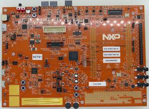
- NXP S32K3X4EVB-Q257 evaluation board: https://wiki.segger.com/NXP_S32K3X4EVB
- NXP XS32K3XXCVB-Q257 evaluation board: https://wiki.segger.com/NXP_XS32K3XXCVB
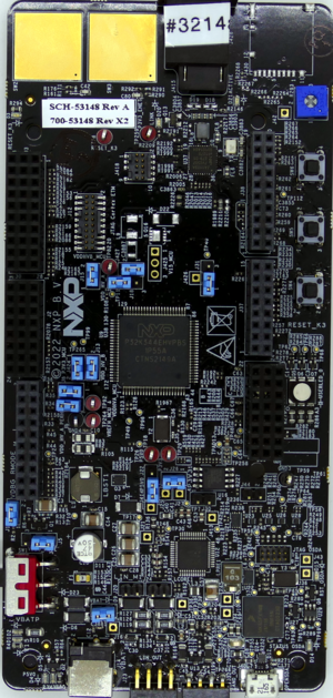
- NXP X32K3XXEVB-Q172 evaluation board: https://wiki.segger.com/NXP_X32K3XXEVB
Example Application
- NXP S32K3X4EVB evaluation board: https://wiki.segger.com/NXP_S32K3X4EVB#Example_Project
The example has been tested on the S32K3X4EVB but it should run on any S32K344 based hardware.
Tracing on NXP S32K344
Minimum requirements
In order to use trace on the NXP S32K344 MCU devices, the following minimum requirements have to be met:
- J-Link software version V7.70c or later
- Ozone V3.26h or later (if streaming trace and / or the sample project from below shall be used)
- J-Trace PRO (for Cortex-M) HW version V1.0 or later for streaming trace
To rebuild the project our IDE Embedded Studio can be used. The recommended version to rebuild the projects is V6.30. But the examples are all prebuild and work out-of-the box with Ozone, so rebuilding is not necessary.
Streaming trace
The project has been tested with the minimum requirements mentioned above and the following two eval board:
- S32K3X4EVB-Q257: NXP_S32K344_TracePins.zip
- S32K3X4EVB-T172: NXP_S32K344_S32K3X4EVB_TracePins.zip
Trace buffer (TMC/ETB)
The project below is utilizing the on-chip trace buffer (it is not meant for streaming trace) and works with any NXP S32K344 board.
- Example project: NXP_S32K344_TraceBuffer.zip
Tested Hardware
Specifics/Limitations
The S32K3X4EVB_T172 needs some solder bridges closed and resistors removed for all 4 trace data pins to work. For more information about this see the board specific schematics.
Reference trace signal quality
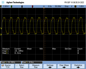
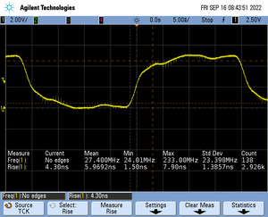
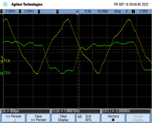
The following pictures show oscilloscope measurements of trace signals output by the NXP S32K3X4EVB-Q257 using the example project. All measurements have been performed using a Agilent InfiniiVision DSO7034B 350 MHz 2GSa/s oscilloscope and 1156A 1.5 GHz Active Probes. If your trace signals look similar on your trace hardware, chances are good that tracing will work out-of-the-box using the example project. More information about correct trace timing can be found at the following website.
Trace clock signal quality
The trace clock signal quality shows multiple trace clock cycles on the tested hardware as reference.
Rise time
The rise time of a signal shows the time needed for a signal to rise from logical 0 to logical 1. For this the values at 10% and 90% of the expected voltage level get used as markers. The following picture shows such a measurement for the trace clock signal.
Setup time
The setup time shows the relative setup time between a trace data signal and trace clock. The measurement markers are set at 50% of the expected voltage level respectively. The following picture shows such a measurement for the trace data signal 0 relative to the trace clock signal.
