Difference between revisions of "OKdo E1"
(Created page with " thumb | right | 450px | OKdo E1 evaluation board This article describes specifics for the ''OKdo E1'' evaluation board, with an NXP LPC55S69JBD100...") |
(→Example Project) |
||
| (One intermediate revision by the same user not shown) | |||
| Line 11: | Line 11: | ||
== Preparing for J-Link == |
== Preparing for J-Link == |
||
| − | + | To make the OKdo E1 evaluation board work with J-Link, it is required to solder connections to the board.<br> |
|
To use SWD, the following is required: |
To use SWD, the following is required: |
||
* As marked in the picture above: |
* As marked in the picture above: |
||
| Line 22: | Line 22: | ||
{| class="wikitable" |
{| class="wikitable" |
||
|- |
|- |
||
| − | ! J-Link pin !! Board connection |
+ | ! J-Link pin !! Board connection (as shown in the picture) |
|- |
|- |
||
| 7 (SWDIO) || 1 (TRGT_SWDIO) |
| 7 (SWDIO) || 1 (TRGT_SWDIO) |
||
| Line 39: | Line 39: | ||
== Example Project == |
== Example Project == |
||
| − | The following example project was created with the SEGGER Embedded Studio project wizard and runs out-of-the-box on the |
+ | The following example project was created with the SEGGER Embedded Studio project wizard and runs out-of-the-box on the OKdo E1 evaluation board. It is a simple ''Hello World'' sample linked into the internal flash.<br> |
[[File:OKdo_E1_Example_ES_V452c.zip | Hello World example]] |
[[File:OKdo_E1_Example_ES_V452c.zip | Hello World example]] |
||
Latest revision as of 17:24, 18 June 2020

This article describes specifics for the OKdo E1 evaluation board, with an NXP LPC55S69JBD100 target MCU.
Minimum requirements
- J-Link software V6.80b or later
- Embedded Studio V4.52c (for the example project)
- J-Link V10 or later / J-Trace PRO V1 or later
Preparing for J-Link
To make the OKdo E1 evaluation board work with J-Link, it is required to solder connections to the board.
To use SWD, the following is required:
- As marked in the picture above:
- Solder a cable in front or behind the resistor R308 (1)(TRGT_SWDIO).
- Solder a cable in front or behind the resistor R307 (2)(TRGT_SWCLK).
- Solder a cable to GND (3).
- Solder a cable to VDD (4).
-
Connect the J-Link pins to corresponding cables as listed in the table below:
J-Link pin Board connection (as shown in the picture) 7 (SWDIO) 1 (TRGT_SWDIO) 9 (SWCLK) 2 (TRGT_SWCLK) 4 (GND) 3 (GND) 1 (VTref) 4 (VDD) For more information about the J-Link interface please refer to the SEGGER homepage
- Power the board via the DEBUG USB port.
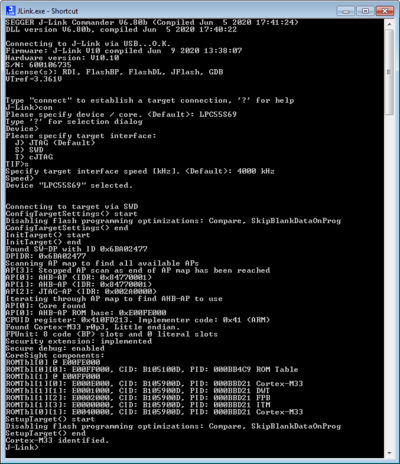
- Verify the Connection with e.g. J-Link Commander. The output should look as follows:

Example Project
The following example project was created with the SEGGER Embedded Studio project wizard and runs out-of-the-box on the OKdo E1 evaluation board. It is a simple Hello World sample linked into the internal flash.
File:OKdo E1 Example ES V452c.zip