OKdo E1
Revision as of 17:20, 18 June 2020 by Fabian (talk | contribs) (Created page with " thumb | right | 450px | OKdo E1 evaluation board This article describes specifics for the ''OKdo E1'' evaluation board, with an NXP LPC55S69JBD100...")

This article describes specifics for the OKdo E1 evaluation board, with an NXP LPC55S69JBD100 target MCU.
Minimum requirements
- J-Link software V6.80b or later
- Embedded Studio V4.52c (for the example project)
- J-Link V10 or later / J-Trace PRO V1 or later
Preparing for J-Link
Do make the OKdo E1 evaluation board work with J-Link, it is required to make the debug interface accessible. To use SWD, the following is required:
- As marked in the picture above:
- Solder a cable in front or behind the resistor R308 (1)(TRGT_SWDIO).
- Solder a cable in front or behind the resistor R307 (2)(TRGT_SWCLK).
- Solder a cable to GND (3).
- Solder a cable to VDD (4).
-
Connect the J-Link pins to corresponding cables as listed in the table below:
J-Link pin Board connection 7 (SWDIO) 1 (TRGT_SWDIO) 9 (SWCLK) 2 (TRGT_SWCLK) 4 (GND) 3 (GND) 1 (VTref) 4 (VDD) For more information about the J-Link interface please refer to the SEGGER homepage
- Power the board via the DEBUG USB port.
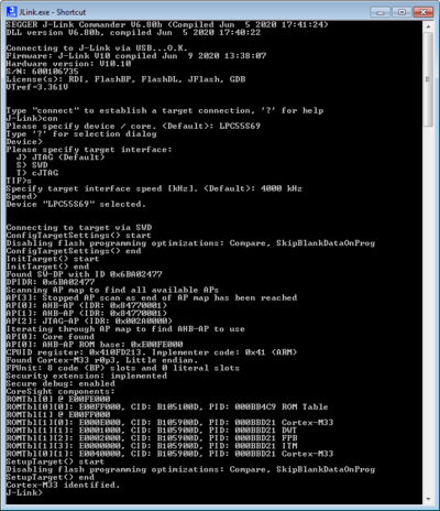
- Verify the Connection with e.g. J-Link Commander. The output should look as follows:

Example Project
The following example project was created with the SEGGER Embedded Studio project wizard and runs out-of-the-box on the NXP JN5189-DK006. It is a simple Hello World sample linked into the internal flash.
File:OKdo E1 Example ES V452c.zip