Difference between revisions of "NXP RD-RW616-BGA IPA-2A/1A"
(→Preparing for J-Link) |
|||
| Line 1: | Line 1: | ||
| + | [[Category:Evalboards]] |
||
__TOC__ |
__TOC__ |
||
Latest revision as of 13:20, 15 May 2024
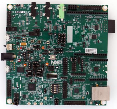
This article describes specifics for the NXP RD-RW616-BGA_IPA-2A/1A evaluation board.

Preparing for J-Link
- Power the board via J1
- Jumper JP1 must be set in order to use J-Link
For use of SWD:
- HD12 1-2 has to be closed (RF_CNTL_2/CON[11])
- Connect JLINK to P2 (SWD)
For use of JTAG:
- HD12 1-2 has to be open (RF_CNTL_2/CON[11])
- Connect JLINK to J19 (JTAG)
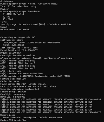
- Verify the Connection with e.g. J-Link Commander. The output should look as follows:
Example Project
The following example project was created with the SEGGER Embedded Studio project wizard and runs out-of-the-box on the NXP RD-RW616-BGA_IPA-2A/1A.
It is a simple Hello World sample linked into the internal flash.
SETUP
- J-Link software: V7.92c
- Embedded Studio: V7.20
- Hardware: NXP RD-RW616-BGA_IPA-2A/1A
- Link: File:NXP RW61x TestProject ES 7V20.zip
