Difference between revisions of "XHSC HC32LF17/9xGO-STK-V2.0"
(Created page with "Category:Evalboards __TOC__ This article describes specifics for the [SiliconVendor] [EvalBoardName] evaluation board.<br> '''[PICTURE OF BOARD]''' File:VENDOR_BOARDNAM...") |
|||
| (2 intermediate revisions by the same user not shown) | |||
| Line 2: | Line 2: | ||
__TOC__ |
__TOC__ |
||
| − | This article describes specifics for the |
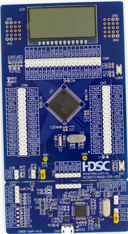
+ | This article describes specifics for the XHSC HC32LF17/9xGO-STK-V2.0 evaluation board.<br> |
| + | [[File:XHSC_HC32LF17-9x GO-STK-V2.0_HC32L196PCTA_board.jpg|450px]] |
||
| − | '''[PICTURE OF BOARD]''' |
||
| − | [[File:VENDOR_BOARDNAME.jpg|450px]] |
||
== Preparing for J-Link == |
== Preparing for J-Link == |
||
| − | *Connect the J-Link to ...... |
||
*Connect the J-Link to this pins: |
*Connect the J-Link to this pins: |
||
{| class="seggertable" |
{| class="seggertable" |
||
| Line 13: | Line 11: | ||
! J-Link Pin || Connector !! Pin || Name |
! J-Link Pin || Connector !! Pin || Name |
||
|- |
|- |
||
| − | | VTref || || || |
+ | | VTref || CN5 || 1 || VDD |
|- |
|- |
||
| − | | GND || || || |
+ | | GND || CN5 || 4 || GND |
|- |
|- |
||
| − | | nTRST || || || |
+ | | nTRST || CN5 || 6 || RSTB |
|- |
|- |
||
| − | | |
+ | | TMS/SWDIO || CN5 || 3 || SWIO |
|- |
|- |
||
| − | | |
+ | | TCK/SWCLK || CN5 || 2 || SWCK |
| − | |- |
||
| − | | TCK/SWCLK || || || |
||
| − | |- |
||
| − | | RTCK || || || |
||
| − | |- |
||
| − | | TDO/SWO || || || |
||
| − | |- |
||
| − | | RESET || || || |
||
| − | |- |
||
| − | | DBGRQ || || || |
||
| − | |- |
||
| − | | 5V-Supply || || || |
||
| − | |||
|} |
|} |
||
| − | *Power the board via |
+ | *Power the board via CN6. |
| + | *The debugger CMSIS-DAP-V1.0 has to be removed. |
||
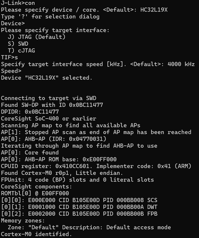
* Verify the Connection with e.g. [https://wiki.segger.com/J-Link_cannot_connect_to_the_CPU#Verify_functionality_using_J-Link_Commander J-Link Commander]. The output should look as follows: |
* Verify the Connection with e.g. [https://wiki.segger.com/J-Link_cannot_connect_to_the_CPU#Verify_functionality_using_J-Link_Commander J-Link Commander]. The output should look as follows: |
||
| + | [[File:XHSC_HC32LF17-9x GO-STK-V2.0_HC32L196PCTA_connect.png|400px]] |
||
| − | '''[PICTURE OF CONNECT]''' |
||
| − | [[File:VENDOR_DEVICE_CONNECT.PNG|400px]] |
||
== Example Project== |
== Example Project== |
||
| − | The following example project was created with the SEGGER Embedded Studio project wizard and runs out-of-the-box on the |
+ | The following example project was created with the SEGGER Embedded Studio project wizard and runs out-of-the-box on the XHSC HC32LF17/9xGO-STK-V2.0.<br> |
| + | It is a simple Hello World sample linked into the internal flash.<br> |
||
====SETUP==== |
====SETUP==== |
||
*Embedded Studio: V7.20 |
*Embedded Studio: V7.20 |
||
| − | *Hardware: |
+ | *Hardware: XHSC HC32LF17/9xGO-STK-V2.0 |
| − | *Link: [[File: |
+ | *Link: [[File:XHSC_HC32L196PCTA_TestProject_ES_V720.zip]] |
Latest revision as of 19:19, 17 June 2024
This article describes specifics for the XHSC HC32LF17/9xGO-STK-V2.0 evaluation board.

Preparing for J-Link
- Connect the J-Link to this pins:
| J-Link Pin | Connector | Pin | Name |
|---|---|---|---|
| VTref | CN5 | 1 | VDD |
| GND | CN5 | 4 | GND |
| nTRST | CN5 | 6 | RSTB |
| TMS/SWDIO | CN5 | 3 | SWIO |
| TCK/SWCLK | CN5 | 2 | SWCK |
- Power the board via CN6.
- The debugger CMSIS-DAP-V1.0 has to be removed.
- Verify the Connection with e.g. J-Link Commander. The output should look as follows:
Example Project
The following example project was created with the SEGGER Embedded Studio project wizard and runs out-of-the-box on the XHSC HC32LF17/9xGO-STK-V2.0.
It is a simple Hello World sample linked into the internal flash.
SETUP
- Embedded Studio: V7.20
- Hardware: XHSC HC32LF17/9xGO-STK-V2.0
- Link: File:XHSC HC32L196PCTA TestProject ES V720.zip
