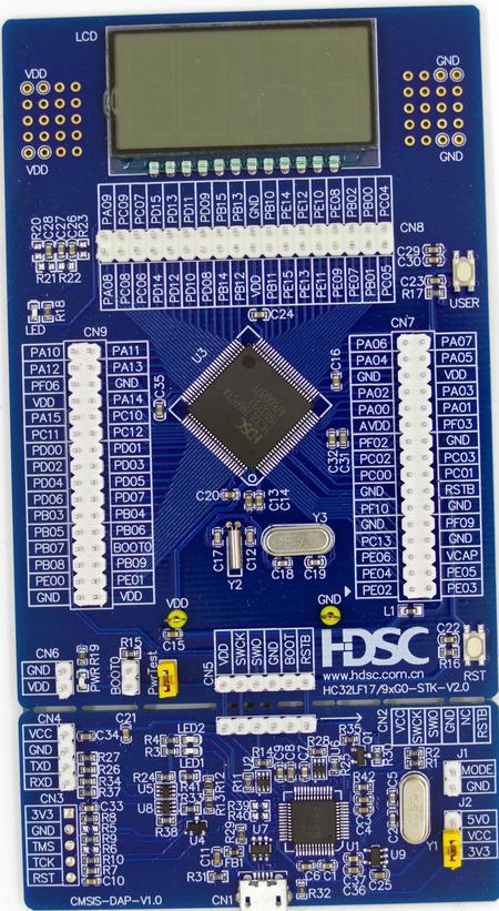
XHSC HC32LF17/9xGO-STK-V2.0
Revision as of 19:19, 17 June 2024 by Torben.scharping (talk | contribs)
This article describes specifics for the XHSC HC32LF17/9xGO-STK-V2.0 evaluation board.

Preparing for J-Link
- Connect the J-Link to this pins:
| J-Link Pin | Connector | Pin | Name |
|---|---|---|---|
| VTref | CN5 | 1 | VDD |
| GND | CN5 | 4 | GND |
| nTRST | CN5 | 6 | RSTB |
| TMS/SWDIO | CN5 | 3 | SWIO |
| TCK/SWCLK | CN5 | 2 | SWCK |
- Power the board via CN6.
- The debugger CMSIS-DAP-V1.0 has to be removed.
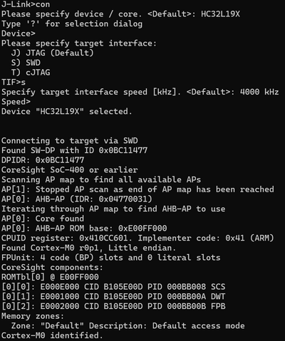
- Verify the Connection with e.g. J-Link Commander. The output should look as follows:
Example Project
The following example project was created with the SEGGER Embedded Studio project wizard and runs out-of-the-box on the XHSC HC32LF17/9xGO-STK-V2.0.
It is a simple Hello World sample linked into the internal flash.
SETUP
- Embedded Studio: V7.20
- Hardware: XHSC HC32LF17/9xGO-STK-V2.0
- Link: File:XHSC HC32L196PCTA TestProject ES V720.zip
