Difference between revisions of "e-peas EDMS105N EVK"
(Created page with "__TOC__ This article describes specifics for the [SiliconVendor] [EvalBoardName] evaluation board.<br> '''[PICTURE OF BOARD]''' 450px == Prepar...") |
(→Preparing for J-Link) |
||
| (3 intermediate revisions by the same user not shown) | |||
| Line 1: | Line 1: | ||
__TOC__ |
__TOC__ |
||
| − | This article describes specifics for the |
+ | This article describes specifics for the e-peas EDMS105N_EVK evaluation board.<br> |
'''[PICTURE OF BOARD]''' |
'''[PICTURE OF BOARD]''' |
||
[[File:VENDOR_BOARDNAME.jpg|450px]] |
[[File:VENDOR_BOARDNAME.jpg|450px]] |
||
== Preparing for J-Link == |
== Preparing for J-Link == |
||
| − | *Connect the J-Link to |
+ | *Connect the J-Link to the following Pins: |
| + | ** GND: CN4.1 |
||
| − | *Power the board via........ |
||
| + | ** VTref: CN5.1 |
||
| + | ** SWDIO: JP7.3 |
||
| + | ** SWCLK_ JP7.1 |
||
| + | ** RESET: JP7.5 |
||
| + | *Power the board via S1. |
||
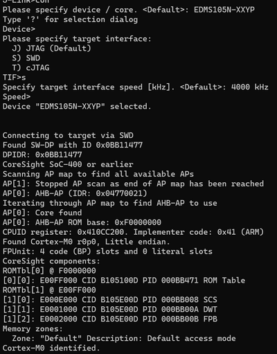
* Verify the Connection with e.g. [https://wiki.segger.com/J-Link_cannot_connect_to_the_CPU#Verify_functionality_using_J-Link_Commander J-Link Commander]. The output should look as follows: |
* Verify the Connection with e.g. [https://wiki.segger.com/J-Link_cannot_connect_to_the_CPU#Verify_functionality_using_J-Link_Commander J-Link Commander]. The output should look as follows: |
||
| + | [[File:Epeas_MDNS105N-xxyP_connect.png|400px]] |
||
| − | '''[PICTURE OF CONNECT]''' |
||
| − | [[File:VENDOR_DEVICE_CONNECT.PNG|400px]] |
||
== Example Project== |
== Example Project== |
||
| − | The following example project was created with the SEGGER Embedded Studio project wizard and runs out-of-the-box on the |
+ | The following example project was created with the SEGGER Embedded Studio project wizard and runs out-of-the-box on the e-peas EDMS105N_EVK.<br>It is a simple Hello World sample linked into the internal flash.<br> |
====SETUP==== |
====SETUP==== |
||
| − | *J-Link software: |
+ | *J-Link software: V7.88k |
| − | *Embedded Studio: |
+ | *Embedded Studio: V6.34 |
| − | *Hardware: |
+ | *Hardware: e-peas EDMS105N_EVK |
| − | *Link: [[File: |
+ | *Link: [[File:Epeas_EDMS105N_TestProject_ES_V634.zip]] |
Revision as of 16:05, 29 June 2023
This article describes specifics for the e-peas EDMS105N_EVK evaluation board.
[PICTURE OF BOARD]
450px
Preparing for J-Link
- Connect the J-Link to the following Pins:
- GND: CN4.1
- VTref: CN5.1
- SWDIO: JP7.3
- SWCLK_ JP7.1
- RESET: JP7.5
- Power the board via S1.
- Verify the Connection with e.g. J-Link Commander. The output should look as follows:
Example Project
The following example project was created with the SEGGER Embedded Studio project wizard and runs out-of-the-box on the e-peas EDMS105N_EVK.
It is a simple Hello World sample linked into the internal flash.
SETUP
- J-Link software: V7.88k
- Embedded Studio: V6.34
- Hardware: e-peas EDMS105N_EVK
- Link: File:Epeas EDMS105N TestProject ES V634.zip
