Difference between revisions of "NXP X-OM2CTN730"
(Created page with "__TOC__ This article describes specifics for the NXP X-OM2CTN730 evaluation board.<br> 450px == Preparing for J-Link == *Connect the J-L...") |
(→Preparing for J-Link) |
||
| Line 5: | Line 5: | ||
== Preparing for J-Link == |
== Preparing for J-Link == |
||
| − | *Connect the J-Link to |
+ | *Connect the J-Link to J302 |
| − | *Power the board via |
+ | *Power the board via J400. |
* Verify the Connection with e.g. [https://wiki.segger.com/J-Link_cannot_connect_to_the_CPU#Verify_functionality_using_J-Link_Commander J-Link Commander]. The output should look as follows: |
* Verify the Connection with e.g. [https://wiki.segger.com/J-Link_cannot_connect_to_the_CPU#Verify_functionality_using_J-Link_Commander J-Link Commander]. The output should look as follows: |
||
[[File:NXP_X-OM2CTN730_CTN730_connect.png|400px]] |
[[File:NXP_X-OM2CTN730_CTN730_connect.png|400px]] |
||
Revision as of 15:20, 20 September 2023
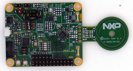
This article describes specifics for the NXP X-OM2CTN730 evaluation board.

Preparing for J-Link
- Connect the J-Link to J302
- Power the board via J400.
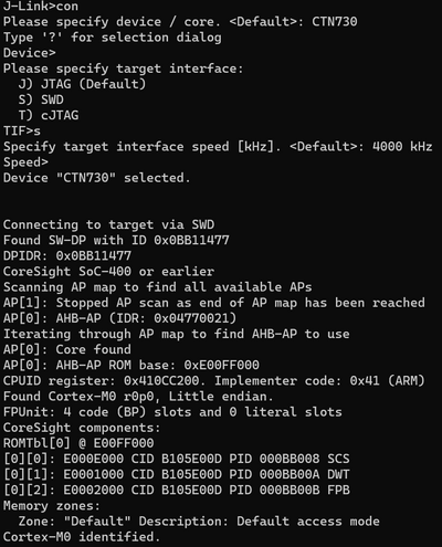
- Verify the Connection with e.g. J-Link Commander. The output should look as follows:
Example Project
The following example project was created with the SEGGER Embedded Studio project wizard and runs out-of-the-box on the NXP X-OM2CTN730.
It is a simple Hello World sample linked into the internal flash.
SETUP
- J-Link software: V7.92g
- Embedded Studio: V7.20
- Hardware: NXP X-OM2CTN730
- Link: File:NXP X-OM2CTN730 CTN730 TestProject ES 7V20.zip
