Difference between revisions of "CFI Flash"
(→J-Flash) |
(→Generic - via J-Link script file) |
||
| Line 14: | Line 14: | ||
*/ |
*/ |
||
int ConfigTargetSettings(void) { |
int ConfigTargetSettings(void) { |
||
| − | JLINK_ExecCommand("SetCFIFlash 0x64000000-0x64FFFFFF"); |
+ | JLINK_ExecCommand("SetCFIFlash 0x64000000-0x64FFFFFF"); // Same command as "SetCFIFlash 0x64000000-0x64FFFFFF, 1, 16" (NumChips = 1, NumBits = 16) |
JLINK_ExecCommand("SetWorkRAM 0x20000000-0x2000FFFF"); |
JLINK_ExecCommand("SetWorkRAM 0x20000000-0x2000FFFF"); |
||
return 0; |
return 0; |
||
| Line 34: | Line 34: | ||
JLINK_TARGET_Halt(); |
JLINK_TARGET_Halt(); |
||
| − | JLINK_ExecCommand("SetCFIFlash 0x64000000-0x64FFFFFF"); |
+ | JLINK_ExecCommand("SetCFIFlash 0x64000000-0x64FFFFFF"); // Same command as "SetCFIFlash 0x64000000-0x64FFFFFF, 1, 16" (NumChips = 1, NumBits = 16) |
JLINK_ExecCommand("SetWorkRAM 0x20000000-0x2000FFFF"); |
JLINK_ExecCommand("SetWorkRAM 0x20000000-0x2000FFFF"); |
||
r |= JLINK_MEM_WriteU32(0x40021014, 0x00000114); // RCC_AHBENR, FSMC clock enable |
r |= JLINK_MEM_WriteU32(0x40021014, 0x00000114); // RCC_AHBENR, FSMC clock enable |
||
Revision as of 12:18, 15 October 2020
The setup for download into CFI-compliant memory is different from the one for internal flash. Initialization of the external memory interface the CFI flash is connected to, is user’s responsibility and is expected by the J-Link software to be done prior to performing accesses to the specified CFI area.
Generic - via J-Link script file
Specifying of the CFI area is done in a J-Link script file, as explained below. The following sample script defines a 16 MiB CFI flash at address 0x64000000 and a 64 KiB WorkRAM at address 0x20000000:
/*********************************************************************
*
*       ConfigTargetSettings
*/
int ConfigTargetSettings(void) {
  JLINK_ExecCommand("SetCFIFlash 0x64000000-0x64FFFFFF"); // Same command as "SetCFIFlash 0x64000000-0x64FFFFFF, 1, 16" (NumChips = 1, NumBits = 16)
  JLINK_ExecCommand("SetWorkRAM 0x20000000-0x2000FFFF");
  return 0;
}
In the following example, it is explained which steps are necessary to prepare J-Link for download into external CFI flash memory based on a sample sequence for a ST STM32F103ZE device:
/*********************************************************************
*
*       SetupTarget
*/
int SetupTarget(void) {
  int r;

  r = 0;

  JLINK_TARGET_Halt();
  JLINK_ExecCommand("SetCFIFlash 0x64000000-0x64FFFFFF"); // Same command as "SetCFIFlash 0x64000000-0x64FFFFFF, 1, 16" (NumChips = 1, NumBits = 16)
  JLINK_ExecCommand("SetWorkRAM 0x20000000-0x2000FFFF");
  r |= JLINK_MEM_WriteU32(0x40021014, 0x00000114); // RCC_AHBENR, FSMC clock enable
  r |= JLINK_MEM_WriteU32(0x40021018, 0x000001FD); // GPIOD~G clock enable
  r |= JLINK_MEM_WriteU32(0x40011400, 0xB4BB44BB); // GPIOD low config, NOE, NWE => Output, NWAIT => Input
  r |= JLINK_MEM_WriteU32(0x40011404, 0xBBBBBBBB); // GPIOD high config, A16-A18
  r |= JLINK_MEM_WriteU32(0x40011800, 0xBBBBBBBB); // GPIOE low config, A19-A23
  r |= JLINK_MEM_WriteU32(0x40011804, 0xBBBBBBBB); // GPIOE high config, D5-D12
  r |= JLINK_MEM_WriteU32(0x40011C00, 0x44BBBBBB); // GPIOF low config, A0-A5
  r |= JLINK_MEM_WriteU32(0x40011C04, 0xBBBB4444); // GPIOF high config, A6-A9
  r |= JLINK_MEM_WriteU32(0x40012000, 0x44BBBBBB); // GPIOG low config, A10-A15
  r |= JLINK_MEM_WriteU32(0x40012004, 0x444B4BB4); // GPIOG high config, NE2 => output
  r |= JLINK_MEM_WriteU32(0xA0000008, 0x00001059); // CS control reg 2, 16-bit, write enable, Type: NOR flash
  r |= JLINK_MEM_WriteU32(0xA000000C, 0x10000505); // CS2 timing reg (read access)
  r |= JLINK_MEM_WriteU32(0xA000010C, 0x10000505); // CS2 timing reg (write access)
  if (r < 0) {
    return -1;
  }
  return 0;
}
J-Flash
- Create a new project
- Select the correct device or at least the core
- Add the device specific initialization of the external memory controller to the J-Flash init steps which are part of the project (Project settings -> MCU -> Init steps).
- Add a new flash bank
- Setup the Base Addr and the Organization of the CFI flash according to your setup.
- Check Automatically detect flash memory
Alternatively the method in the beginning of this article (Generic - via J-Link script file) can be used to initialize the CPU.
[Deprecated] Via J-Link settings file
- Open the J-Link settings file (see J-Link settings file)
- Add the following lines to the file
[CFI]
CFISize = <FlashSize>
CFIAddr = <FlashAddr>
[GENERAL]
WorkRAMSize = <RAMSize>
WorkRAMAddr = <RAMAddr>
- After this the file should look similar to the sample in the following screenshot.
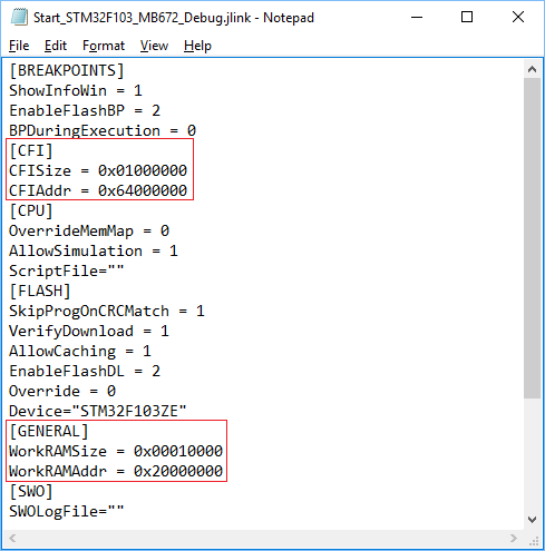
- Save the settings file and restart the debug session.
