Difference between revisions of "ArteryTek AT-START-F403A"
m (Torben.scharping moved page Artery AT-START-F403 to Artery AT-START-F403A) |
|||
| Line 10: | Line 10: | ||
! J-Link Pin || Connector !! Pin || Name |
! J-Link Pin || Connector !! Pin || Name |
||
|- |
|- |
||
| − | | VTref || J1 || |
+ | | VTref || J1 || 23 || VDD |
|- |
|- |
||
| − | | GND || J1 || |
+ | | GND || J1 || 22 || GND |
|- |
|- |
||
| − | | TDI || J1 || |
+ | | TDI || J1 || 25 || PA15 |
|- |
|- |
||
| − | | TMS/SWDIO || J1 || |
+ | | TMS/SWDIO || J1 || 20|| PA13 |
|- |
|- |
||
| − | | TCK/SWCLK || J1 || |
+ | | TCK/SWCLK || J1 || 24 || PA14 |
|- |
|- |
||
| − | | TDO/SWO || J1 || |
+ | | TDO/SWO || J1 || 37|| PB3 |
|- |
|- |
||
| − | | RESET || |
+ | | RESET || J2 || 14 || NRST |
|} |
|} |
||
*Power the board via CN4. |
*Power the board via CN4. |
||
Revision as of 15:46, 7 February 2024
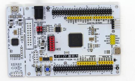
This article describes specifics for the Artery AT-START-F403A evaluation board.

Preparing for J-Link
- Connect the J-Link to this pins:
| J-Link Pin | Connector | Pin | Name |
|---|---|---|---|
| VTref | J1 | 23 | VDD |
| GND | J1 | 22 | GND |
| TDI | J1 | 25 | PA15 |
| TMS/SWDIO | J1 | 20 | PA13 |
| TCK/SWCLK | J1 | 24 | PA14 |
| TDO/SWO | J1 | 37 | PB3 |
| RESET | J2 | 14 | NRST |
- Power the board via CN4.
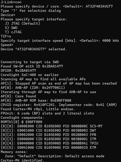
- Verify the Connection with e.g. J-Link Commander. The output should look as follows:
Example Project
The following example project was created with the SEGGER Embedded Studio project wizard and runs out-of-the-box on the Artery AT-START-F403A.
It is a simple Hello World sample linked into the internal flash.
SETUP
- J-Link software: V7.94i
- Embedded Studio: V7.20
- Hardware: Artery AT-START-F403A
- Link: File:Artery AT-START-F403A AT32F403AVGT7 TestProject ES 7V20.zip
