Difference between revisions of "CEC1702 clicker"
| (9 intermediate revisions by 2 users not shown) | |||
| Line 1: | Line 1: | ||
__TOC__ |
__TOC__ |
||
| + | The CEC1702 clicker is a compact development board with a Microchip CEC1702 - a 32-bit ARM® Cortex™ -M4 Processor Core, designed for cryptographic operations. For further information please visit: https://shop.mikroe.com/clicker-cec1702 |
||
| − | This article describes device specifics of the Microchip CEC1702 series devices. |
||
| − | == |
+ | ==Connecting J-Link to the clicker board== |
The Mikroe CEC1702 clicker board does not come with an external debug connector. |
The Mikroe CEC1702 clicker board does not come with an external debug connector. |
||
| Line 9: | Line 9: | ||
# Populate the header J1 (Marked red in attached picture) with a 2 x 5 pin header by soldering |
# Populate the header J1 (Marked red in attached picture) with a 2 x 5 pin header by soldering |
||
| − | # Connect your JLink debug probe with e.g. jumper wires with header J1 the following |
+ | # Connect your JLink debug probe with e.g. jumper wires with header J1 like described in the following table and attached connector picture (Pin 1 is marked with a white dot): |
{| class="wikitable" |
{| class="wikitable" |
||
| Line 15: | Line 15: | ||
! Pin header J1 !! J-Link |
! Pin header J1 !! J-Link |
||
|- |
|- |
||
| − | | Pin 1 ( |
+ | | Pin 1 (RED) || Pin 1 (VTref) |
|- |
|- |
||
| − | | Pin |
+ | | Pin 2 (GREEN) || Pin 7 (SWDIO) |
|- |
|- |
||
| − | | Pin |
+ | | Pin 3 || Do not connect, leave open |
|- |
|- |
||
| − | | Pin |
+ | | Pin 4 (YELLOW) || Pin 9 (SWCLK) |
|- |
|- |
||
| − | | Pin |
+ | | Pin 5 || Do not connect, leave open |
|- |
|- |
||
| − | | Pin 6 |
+ | | Pin 6 || Do not connect, leave open |
|- |
|- |
||
| − | | Pin |
+ | | Pin 7 || Do not connect, leave open |
|- |
|- |
||
| − | | Pin |
+ | | Pin 8 || Do not connect, leave open |
| + | |- |
||
| + | | Pin 9 (BLACK) || Pin 4 (GND) |
||
| + | |- |
||
| + | | Pin 10 (BLUE) || Pin 15 (RESET) |
||
|} |
|} |
||
| − | + | {{Note|The CEC1702 MCU is only connected via SWD on this particular board even though the signals are named "JTAG" in the schematics so make sure to connect through SWD.}} |
|
| + | ==Board specifics== |
||
| − | connect through SWD. |
||
| + | ===Flash programming=== |
||
| + | The CEC1702 does not provide internal (on-chip) flash. On the CEC1702 clicker board there is a serial NOR flash memory (Microchip SST26VF016B) mounted. The CEC1702 boots from this flash. J-Link software version V6.16h or later is needed to program the serial NOR flash. |
||
| + | ==Attachments== |
||
[[File:CEC1702.png|left|thumb|Mikroe CEC1702 clicker]] |
[[File:CEC1702.png|left|thumb|Mikroe CEC1702 clicker]] |
||
| + | [[File:CEC1702_Connector.jpg|left|thumb|Mikroe CEC1702 clicker connector]] |
||
Latest revision as of 15:27, 18 October 2021
Contents
The CEC1702 clicker is a compact development board with a Microchip CEC1702 - a 32-bit ARM® Cortex™ -M4 Processor Core, designed for cryptographic operations. For further information please visit: https://shop.mikroe.com/clicker-cec1702
Connecting J-Link to the clicker board
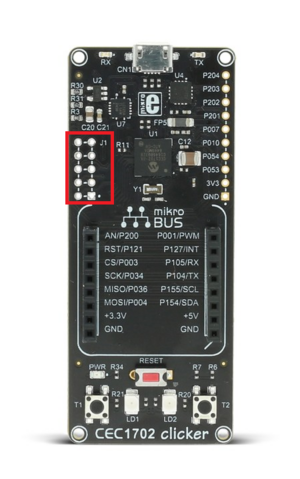
The Mikroe CEC1702 clicker board does not come with an external debug connector. Therefore in order to use an external debug probe like the J-Link the Mikroe CEC1702 clicker board needs to be manually setup:
- Populate the header J1 (Marked red in attached picture) with a 2 x 5 pin header by soldering
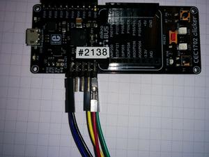
- Connect your JLink debug probe with e.g. jumper wires with header J1 like described in the following table and attached connector picture (Pin 1 is marked with a white dot):
| Pin header J1 | J-Link |
|---|---|
| Pin 1 (RED) | Pin 1 (VTref) |
| Pin 2 (GREEN) | Pin 7 (SWDIO) |
| Pin 3 | Do not connect, leave open |
| Pin 4 (YELLOW) | Pin 9 (SWCLK) |
| Pin 5 | Do not connect, leave open |
| Pin 6 | Do not connect, leave open |
| Pin 7 | Do not connect, leave open |
| Pin 8 | Do not connect, leave open |
| Pin 9 (BLACK) | Pin 4 (GND) |
| Pin 10 (BLUE) | Pin 15 (RESET) |
Note:
The CEC1702 MCU is only connected via SWD on this particular board even though the signals are named "JTAG" in the schematics so make sure to connect through SWD.
The CEC1702 MCU is only connected via SWD on this particular board even though the signals are named "JTAG" in the schematics so make sure to connect through SWD.
Board specifics
Flash programming
The CEC1702 does not provide internal (on-chip) flash. On the CEC1702 clicker board there is a serial NOR flash memory (Microchip SST26VF016B) mounted. The CEC1702 boots from this flash. J-Link software version V6.16h or later is needed to program the serial NOR flash.

