Difference between revisions of "GigaDevice GD32330C-START"
(Created page with "__TOC__ This article describes specifics for the GigaDevice GD32330C-START evaluation board.<br> 450px == Preparing fo...") |
(→Preparing for J-Link) |
||
| Line 10: | Line 10: | ||
! J-Link Pin || Connector !! Pin || Name |
! J-Link Pin || Connector !! Pin || Name |
||
|- |
|- |
||
| − | | VTref || |
+ | | VTref || JP2 || 19 || +3V3 |
|- |
|- |
||
| − | | GND || |
+ | | GND || JP2 || 20 || GND |
|- |
|- |
||
| − | | TMS/SWDIO || |
+ | | TMS/SWDIO || JP2 || 4 || PA13 |
|- |
|- |
||
| − | | TCK/SWCLK || JP3 || |
+ | | TCK/SWCLK || JP3 || 7 || PA14 |
|} |
|} |
||
*Power the board via CN100. |
*Power the board via CN100. |
||
* Verify the Connection with e.g. [https://wiki.segger.com/J-Link_cannot_connect_to_the_CPU#Verify_functionality_using_J-Link_Commander J-Link Commander]. The output should look as follows: |
* Verify the Connection with e.g. [https://wiki.segger.com/J-Link_cannot_connect_to_the_CPU#Verify_functionality_using_J-Link_Commander J-Link Commander]. The output should look as follows: |
||
| − | [[File: |
+ | [[File:GigaDevice_GD32330C-START_GD32330CB_connect.png|400px]] |
== Example Project== |
== Example Project== |
||
Revision as of 16:44, 27 February 2024
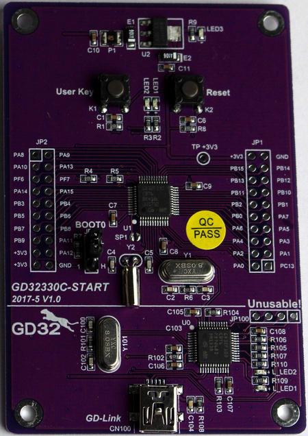
This article describes specifics for the GigaDevice GD32330C-START evaluation board.

Preparing for J-Link
- Connect the J-Link to this pins:
| J-Link Pin | Connector | Pin | Name |
|---|---|---|---|
| VTref | JP2 | 19 | +3V3 |
| GND | JP2 | 20 | GND |
| TMS/SWDIO | JP2 | 4 | PA13 |
| TCK/SWCLK | JP3 | 7 | PA14 |
- Power the board via CN100.
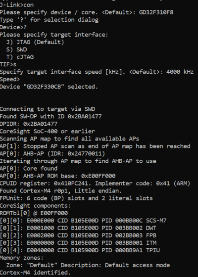
- Verify the Connection with e.g. J-Link Commander. The output should look as follows:
Example Project
The following example project was created with the SEGGER Embedded Studio project wizard and runs out-of-the-box on the GigaDevice GD32F303B-START.
It is a simple Hello World sample linked into the internal flash.
SETUP
- J-Link software: V7.94k
- Embedded Studio: V7.20
- Hardware: GigaDevice GD32F303B-START
- Link: File:GigaDevice GD32F303B-START GD32F303CB TestProject ES 7V20.zip
