Difference between revisions of "GigaDevice GD32350C-START"
| Line 2: | Line 2: | ||
This article describes specifics for the GigaDevice GD32350C-START evaluation board.<br> |
This article describes specifics for the GigaDevice GD32350C-START evaluation board.<br> |
||
| − | [[File:GigaDevice_GD32350C- |
+ | [[File:GigaDevice_GD32350C-START_GD32350C8_board.jpg|450px]] |
== Preparing for J-Link == |
== Preparing for J-Link == |
||
Revision as of 13:33, 3 April 2024
This article describes specifics for the GigaDevice GD32350C-START evaluation board.
450px
Preparing for J-Link
- Connect the J-Link to this pins:
| J-Link Pin | Connector | Pin | Name |
|---|---|---|---|
| VTref | JP2 | 19 | +3V3 |
| GND | JP2 | 20 | GND |
| TMS/SWDIO | JP2 | 4 | PA13 |
| TCK/SWCLK | JP2 | 7 | PA14 |
- Power the board via CN1.
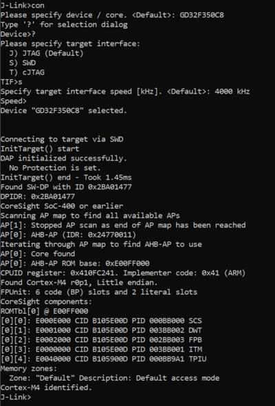
- Verify the Connection with e.g. J-Link Commander. The output should look as follows:
Example Project
The following example project was created with the SEGGER Embedded Studio project wizard and runs out-of-the-box on the GigaDevice GD32350C-START.
It is a simple Hello World sample linked into the internal flash.
SETUP
- Embedded Studio: V7.12a
- Hardware: GigaDevice GD32350C-START
- Link: File:GigaDevice GD32F350C8 TestProject ES V810b.zip
