Difference between revisions of "GigaDevice GD32350R-EVAL"
| (5 intermediate revisions by the same user not shown) | |||
| Line 1: | Line 1: | ||
__TOC__ |
__TOC__ |
||
| − | This article describes specifics for the GigaDevice |
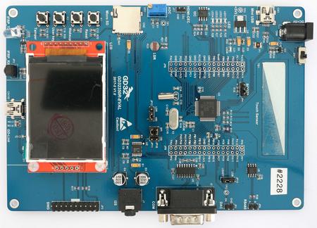
+ | This article describes specifics for the GigaDevice GD32350R-EVAL evaluation board.<br> |
[[File:GigaDevice_GD32350R-EVAL_GD32F350RB_board.jpg|450px]] |
[[File:GigaDevice_GD32350R-EVAL_GD32F350RB_board.jpg|450px]] |
||
== Preparing for J-Link == |
== Preparing for J-Link == |
||
| − | *Connect the J-Link to |
+ | *Connect the J-Link to the JTAG header (JP3) |
| + | *Power the board via CN1. |
||
| − | {| class="seggertable" |
||
| − | |- |
||
| − | ! J-Link Pin || Connector !! Pin || Name |
||
| − | |- |
||
| − | | VTref || JP1 || 4 || +3V3 |
||
| − | |- |
||
| − | | GND || JP1 || 3 || GND |
||
| − | |- |
||
| − | | TMS/SWDIO || JP1 || 2 || IO |
||
| − | |- |
||
| − | | TCK/SWCLK || JP1 || 1 || CK |
||
| − | |} |
||
| − | *Power the board via CN100. |
||
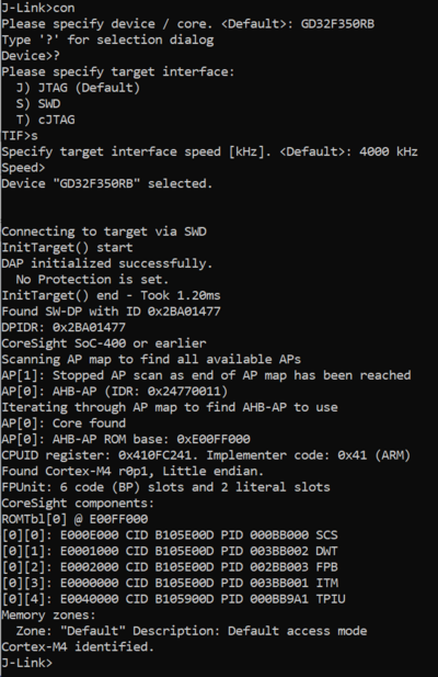
* Verify the Connection with e.g. [https://wiki.segger.com/J-Link_cannot_connect_to_the_CPU#Verify_functionality_using_J-Link_Commander J-Link Commander]. The output should look as follows: |
* Verify the Connection with e.g. [https://wiki.segger.com/J-Link_cannot_connect_to_the_CPU#Verify_functionality_using_J-Link_Commander J-Link Commander]. The output should look as follows: |
||
| − | [[File: |
+ | [[File:GigaDevice_GD32350R-EVAL_GD32F350RB_connect.png|400px]] |
== Example Project== |
== Example Project== |
||
| − | The following example project was created with the SEGGER Embedded Studio project wizard and runs out-of-the-box on the GigaDevice |
+ | The following example project was created with the SEGGER Embedded Studio project wizard and runs out-of-the-box on the GigaDevice GD32350R-EVAL.<br>It is a simple Hello World sample linked into the internal flash.<br> |
====SETUP==== |
====SETUP==== |
||
| − | *Embedded Studio: |
+ | *Embedded Studio: V8.10a |
*Hardware: GigaDevice GD32350R-EVAL |
*Hardware: GigaDevice GD32350R-EVAL |
||
| − | *Link: [[File: |
+ | *Link: [[File:GigaDevice_GD32F350RB_TestProject_ES_V810a.zip]] |
Latest revision as of 14:26, 3 April 2024
This article describes specifics for the GigaDevice GD32350R-EVAL evaluation board.

Preparing for J-Link
- Connect the J-Link to the JTAG header (JP3)
- Power the board via CN1.
- Verify the Connection with e.g. J-Link Commander. The output should look as follows:
Example Project
The following example project was created with the SEGGER Embedded Studio project wizard and runs out-of-the-box on the GigaDevice GD32350R-EVAL.
It is a simple Hello World sample linked into the internal flash.
SETUP
- Embedded Studio: V8.10a
- Hardware: GigaDevice GD32350R-EVAL
- Link: File:GigaDevice GD32F350RB TestProject ES V810a.zip
