Difference between revisions of "Infineon CY-SD2220"
(→SETUP) |
|||
| (One intermediate revision by the same user not shown) | |||
| Line 19: | Line 19: | ||
It is a simple Hello World sample linked into the internal flash.<br> |
It is a simple Hello World sample linked into the internal flash.<br> |
||
====SETUP==== |
====SETUP==== |
||
| − | *J-Link software: V7. |
+ | *J-Link software: V7.94k |
*Embedded Studio: V7.20 |
*Embedded Studio: V7.20 |
||
*Hardware: Infineon CY-SD2220 |
*Hardware: Infineon CY-SD2220 |
||
| − | *Link: [[File: |
+ | *Link: [[File:Infineon_CY-SD2220_Rev01_CYPD7191-40LDXS_TestProject_ES_7V20.zip]] |
Revision as of 10:56, 22 February 2024
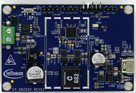
This article describes specifics for the Infineon CY-SD2220 evaluation board.

Preparing for J-Link
- Connect the J-Link to J18:
- GND on J18.2
- SWDIO on J18.5
- SWCLK on J18.4
- Reset on J18.3
- VTref on TP13
- Power the board via J5.
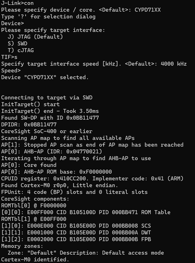
- Verify the Connection with e.g. J-Link Commander. The output should look as follows:
Example Project
The following example project was created with the SEGGER Embedded Studio project wizard and runs out-of-the-box on the Infineon CY-SD2220.
It is a simple Hello World sample linked into the internal flash.
SETUP
- J-Link software: V7.94k
- Embedded Studio: V7.20
- Hardware: Infineon CY-SD2220
- Link: File:Infineon CY-SD2220 Rev01 CYPD7191-40LDXS TestProject ES 7V20.zip
