Difference between revisions of "Renesas EK-RA2A2"
(→SETUP) |
|||
| (2 intermediate revisions by the same user not shown) | |||
| Line 25: | Line 25: | ||
The following example project was created with the SEGGER Embedded Studio project wizard and runs out-of-the-box on the Renesas EK-RA2A2.<br>It is a simple Hello World sample linked into the internal flash.<br> |
The following example project was created with the SEGGER Embedded Studio project wizard and runs out-of-the-box on the Renesas EK-RA2A2.<br>It is a simple Hello World sample linked into the internal flash.<br> |
||
====SETUP==== |
====SETUP==== |
||
| − | *Embedded Studio: |
+ | *Embedded Studio: V8.10 |
*Hardware: Renesas EK-RA2A2 |
*Hardware: Renesas EK-RA2A2 |
||
| − | * |
+ | *[[File:Renesas_R7FA2A2AD_TestProject_ES_V810.zip]] |
Latest revision as of 13:43, 2 April 2024
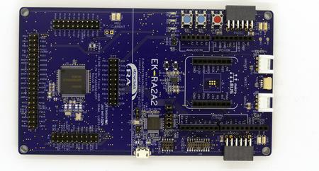
This article describes specifics for the Renesas EK-RA2A2 evaluation board.

Preparing for J-Link
- Connect the J-Link to this pins:
| J-Link Pin | Connector | Pin | Name |
|---|---|---|---|
| VTref | J2 | 1 | VCC |
| GND | J2 | 20 | VSS |
| TMS/SWDIO | J2 | 18 | P108/SWDIO |
| TCK/SWCLK | J2 | 17 | P300/SWCLK |
- Power the board via J10.
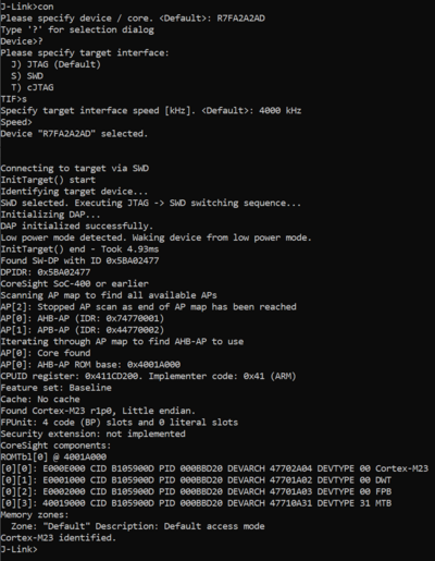
- Verify the Connection with e.g. J-Link Commander. The output should look as follows:
Example Project
The following example project was created with the SEGGER Embedded Studio project wizard and runs out-of-the-box on the Renesas EK-RA2A2.
It is a simple Hello World sample linked into the internal flash.
SETUP
- Embedded Studio: V8.10
- Hardware: Renesas EK-RA2A2
- File:Renesas R7FA2A2AD TestProject ES V810.zip
