Difference between revisions of "STM32VLDISCOVERY"
| Line 24: | Line 24: | ||
The result should be looking like this: |
The result should be looking like this: |
||
| − | [[File: |
+ | [[File:STM32VLDISCOVERY_wired.jpg | 300px | ST STM32VLDISCOVERY wired with jumper cables]] |
| + | [[File:STM32VLDISCOVERY_wired2.jpg | 300px | ST STM32VLDISCOVERY wired with jumper cables]] |
||
*Power the board via (Mini USB) |
*Power the board via (Mini USB) |
||
Revision as of 14:34, 11 August 2023
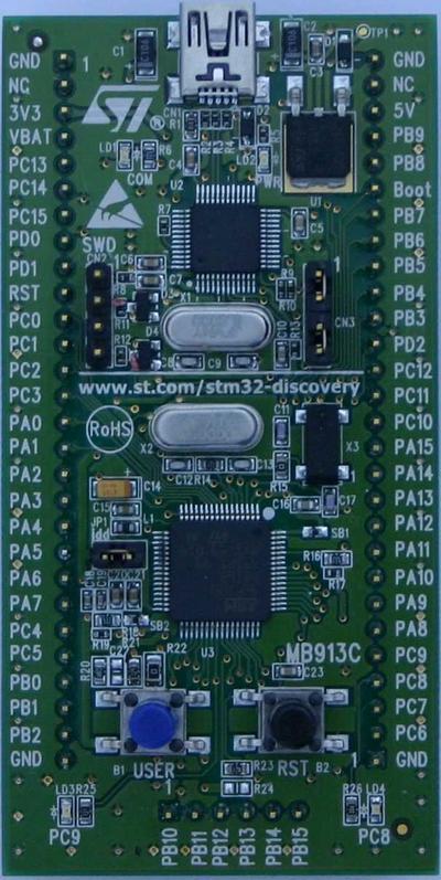
This article describes specifics for the ST STM32VLDISCOVERY board.

Preparing for J-Link
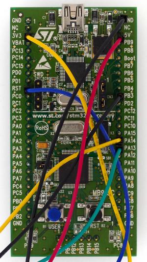
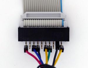
- Connect the board with jumping wires to your J-Link (see table below)
For information about the J-Link pinout please refer to the following page: J-Link SWD pinout.
| J-Link 20 pin debug interface | Pin on evaluation board |
|---|---|
| Pin 1 (VTref, red) | Pin 16 at CN7 pin header |
| Pin 4 (GND, black) | Pin 8 at CN7 pin header |
| Pin 7 (SWDIO, green) | Pin 4 at CN4 pin header |
| Pin 9 (SWCLK, yellow) | Pin 2 at CN4 pin header |
| Pin 15 (RESET, blue) | Pin 5 at CN4 pin header |
The result should be looking like this:
- Power the board via (Mini USB)
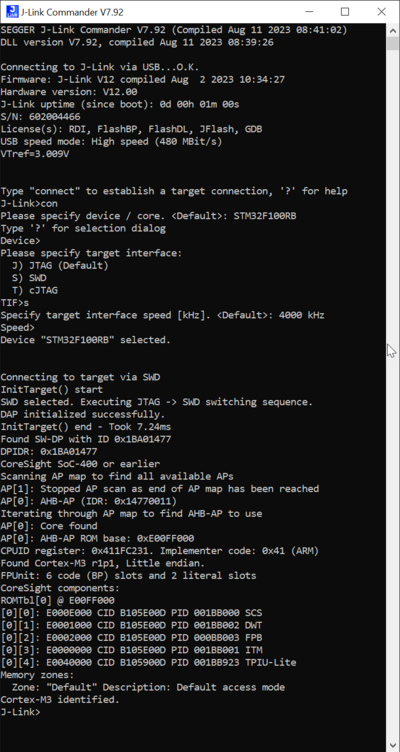
- Verify the Connection with e.g. J-Link Commander. The output should look as follows:
- Note select device: "".
Example Project
The following example project was created with the SEGGER Embedded Studio project wizard and runs out-of-the-box on the ST STM32VLDISCOVERY.
It is a simple Hello World sample linked into the internal flash.
SETUP
- J-Link software: V7.90
- Embedded Studio: V7.20
- Hardware: ST NUCLEO-F103RB
- Link: File:STM32VLDISCOVERY.zip


