File list
This special page shows all uploaded files.
| Date | Name | Thumbnail | Size | Description | Versions |
|---|---|---|---|---|---|
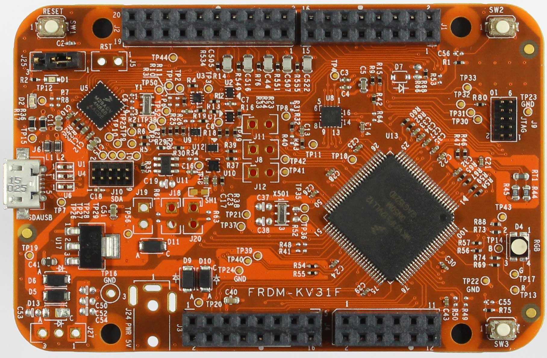
| 09:31, 23 August 2021 | FRDM-KV31F.jpg (file) |  |
267 KB | Evalboard FRDM-KV31F | 1 |
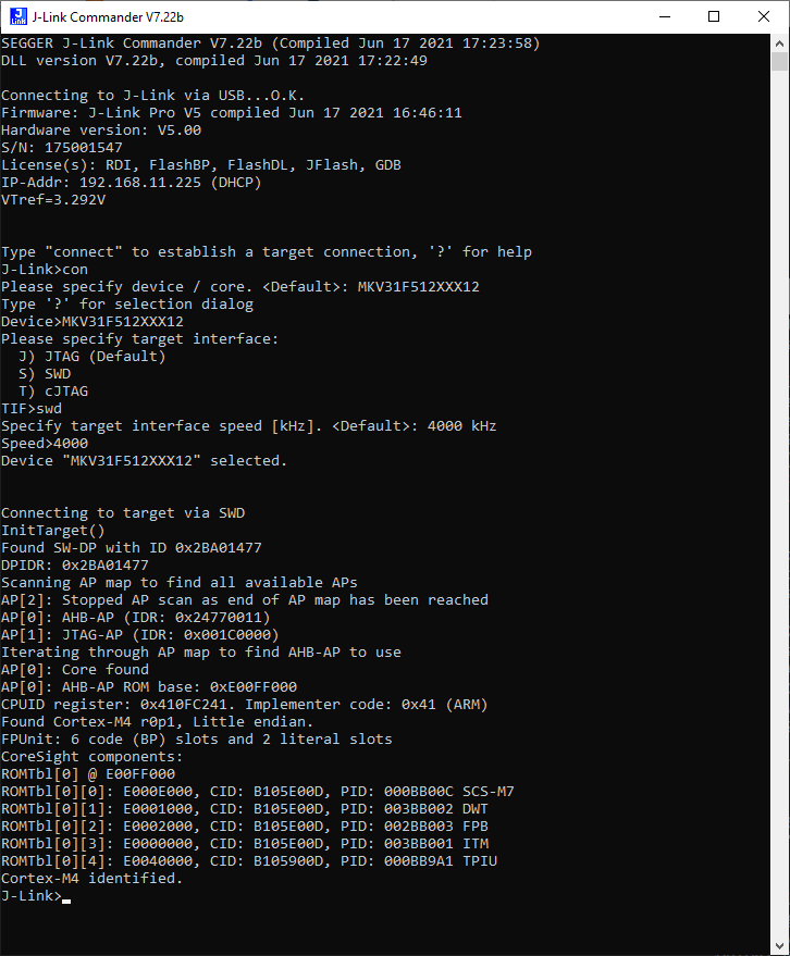
| 10:44, 23 August 2021 | KV31F J-LinkCLI.png (file) |  |
50 KB | 2 | |
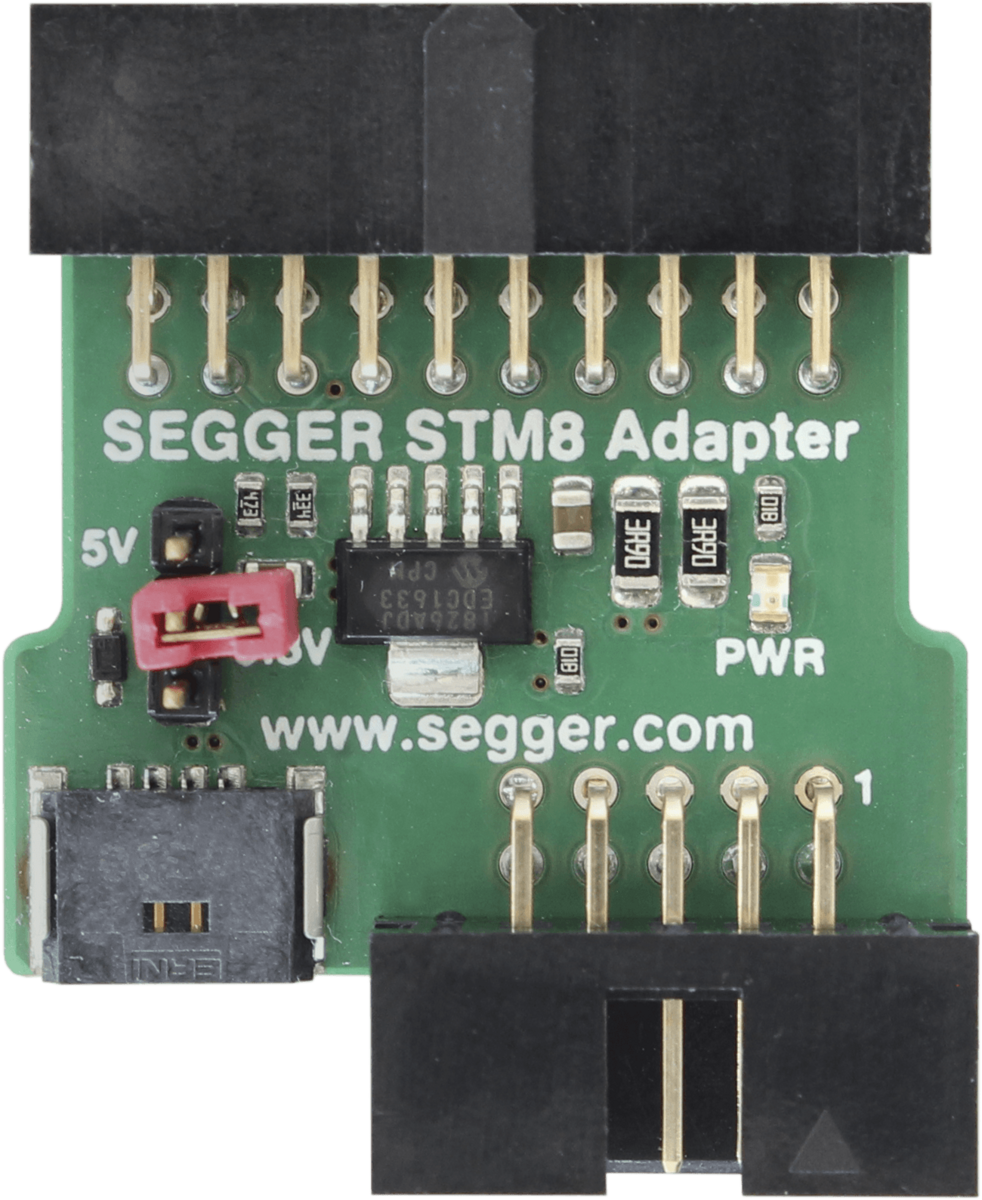
| 10:15, 7 October 2021 | STM8-Adapter.png (file) |  |
1.42 MB | Shows the STM8 Adapter | 1 |
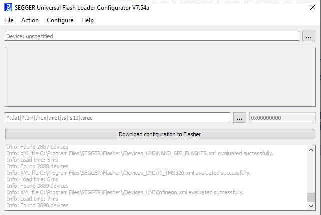
| 10:40, 7 October 2021 | Universal Flash Loader.jpg (file) |  |
76 KB | Shows the empty UFL as example | 1 |
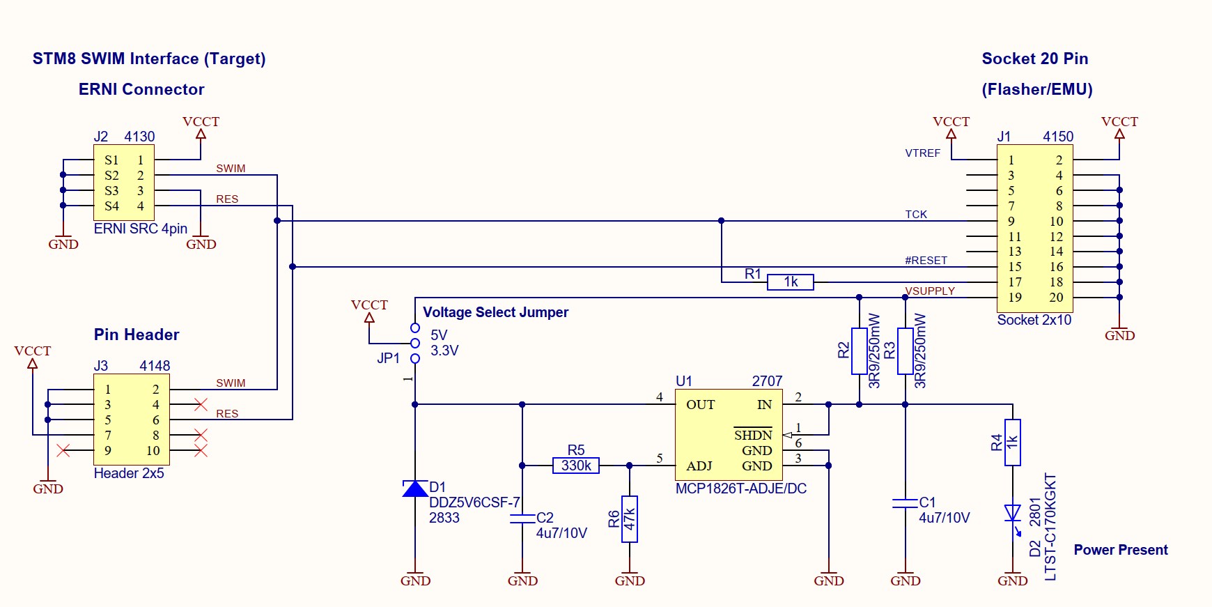
| 09:50, 12 October 2021 | STM8-Adapter-Schematic.jpg (file) |  |
145 KB | Shows the connection diagram of the Stm8 Adapter | 1 |
| 17:00, 29 November 2021 | NXP FRDM-KV31F TestProject ES V568.zip (file) | 16 KB | 1 | ||
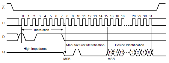
| 12:16, 8 December 2022 | SPI Connect.png (file) |  |
15 KB | S=CS C=SLK D=SI Q=SO | 1 |
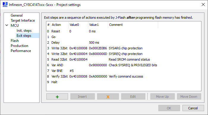
| 10:56, 30 November 2023 | Wiki-Cypress CY8C4xxx CYBLExxxx ProtectCPU.png (file) |  |
25 KB | Corrected exit steps. Image now contain the actual securing steps. | 3 |
| 10:58, 30 November 2023 | Wiki-Cypress PSoC-BL ProtectCPU.png (file) |  |
35 KB | Align design with other screenshot. | 3 |
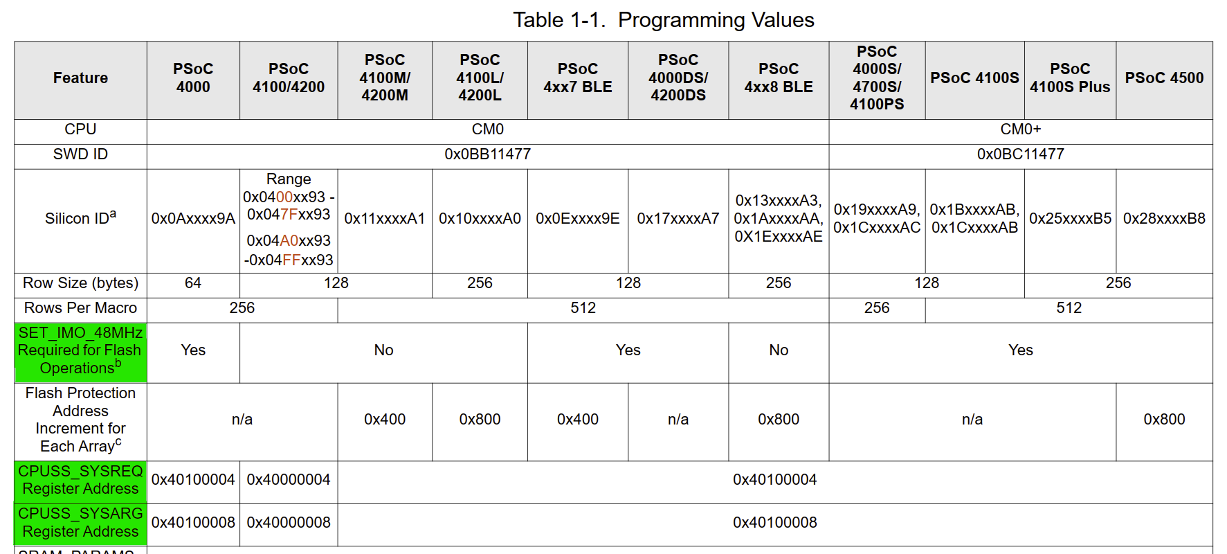
| 11:25, 30 November 2023 | Infineon PSoC ProgrammingSpecifications.png (file) |  |
242 KB | Programming specifications of the PSoC family. The lines marked in green are important: The first line describes whether the IMO must be activated in order to lock the device. The second and third lines contain the addresses of the registers that are u... | 1 |
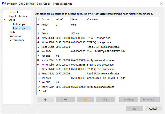
| 11:32, 30 November 2023 | Infineon CY8C4147xxx-Sxxx.jflash (file) | 3 KB | Example project for PSoC family: Exit Steps are set lock the device. | 2 | |
| 11:32, 30 November 2023 | Infineon CY8C4147xxx-Sxxx Clock.jflash (file) | 4 KB | Example project for PSoC family: Exit Steps are set to activate the IMO (Integrated Main Clock) and lock the device. | 1 |