LPC540xx
The LPC540xx series devices are flashless Cortex-M4 based IoT devices. They always boot from external memory (usually QSPI flash).
Contents
Debug scenarios
On the LPC540xx series there are different debug scenarios:
- Debugger downloads to QSPI area and debugs in QSPI area. NXP calls this "XIP debug"
- Debugger downloads to SRAMX area and debugs in SRAMX area. NXP calls this "SRAMX only debug"
- Debugger downloads to SRAMX area but wants QSPI to be programmed. NXP calls this "plain load debug"
Requirements
There are some requirements that need to be fulfilled in order to debug on the LPC540xx series:
- Min. J-Link software V6.31h (beta) or V6.32 (release) is needed. Other versions are not guaranteed to work.
SRAMX only debug
In this scenario, the application is linked to SRAMX and also executed there. When debugging this scenario, the application needs to be re-downloaded on each reset because the LPC540xx device clears the SRAMX on each reset. J-Link supports an IDE independent method to allow an automatic restore of a given memory area, on reset.
Debugger specifics
IAR EWARM
- Make sure that under Project options -> Debugger -> Download the "Use flash loader(s)" checkbox is not checked.* Make sure that a decent target interface speed is used
- Make sure that a restore area is registered under Project options -> Debugger -> Extra Options
--jlink_exec_command MemPreserveOnReset 0x0 0x30000" - Everything else (reset strategy etc.) can stay at defaults
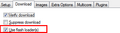
Use flash loader checkbox
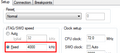
Decent speed
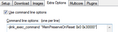
Preserve area

XIP debug
This scenario is easy and straight forward: The application is linked to the QSPI flash area, downloaded to there and also executed there. There are usually no special steps that need to be considered.
Debugger specifics
IAR EWARM
- Make sure that under Project options -> Debugger -> Download the "Use flash loader(s)" checkbox is not checked.
This will make sure that instead of the IAR flash loader, the J-Link one is used, which dynamically detects the QSPI flash that is mounted and supports a broad range of flashes: List of supported QSPI flashes - Make sure that a decent target interface speed is used
- Everything else (reset strategy etc.) can stay at defaults
Use flash loader checkbox
Decent speed
Plain load debug
This scenario is the most complex one because the debugger tells J-Link to download to the SRAMX area but in reality wants the QSPI flash to be programmed. The ROM BTL of the LPC540xx device will copy over QSPI flash data into SRAMX at the next reset. Debugging happens in the SRAMX area. To support this mode, it is required to tell J-Link to handle a write to the SRAMX area as a write to the QSPI flash. J-Link supports in IDE independent method for this.
Debugger specifics
General
- The max. image size that may be debugged with this scenario is the size of the SRAMX
- J-Link will be able to download bigger images but debugging will not work because the ROM BTL of the LPC540x device will only copy up to SRAMX size from the QSPI to SRAMX on boot.
- It is highly recommended to limit the image size to the size of SRAMX by setting the size of code + const to SRAMX size, to be already informed of a possible problem by a linker error, instead of running into weird effects at runtime (only half of the application being copied to SRAMX, which may lead to all kinds of problems and target application crashes)
IAR EWARM
- Make sure that under Project options -> Debugger -> Download the "Use flash loader(s)" checkbox is not checked.
This will make sure that instead of the IAR flash loader, the J-Link one is used, which dynamically detects the QSPI flash that is mounted and supports a broad range of flashes: List of supported QSPI flashes - Make sure that a decent target interface speed is used
- Make sure that an alias area is registered under Project options -> Debugger -> Extra Options
--jlink_exec_command "map add 0x00000000-0x0002FFFF A FLASH 0x10000000 0x1002FFFF" - Everything else (reset strategy etc.) can stay at defaults
Use flash loader checkbox
Decent speed
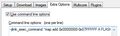
Alias area
SWO
To be able to use the SWO pin, target specific steps have to be executed. The following pins can be initialized as SWO pins:
- PIO0_8
- PIO0_10
Since V6.63b of the J-Link Software and Documentation Pack, SWO for PIO0_10 is supported and works out-of-the-box. If you want to use PIO0_08 as SWO pin, please contact SEGGER support via Support Ticket System.
SWO sample project
The following SWO sample project was tested on the NXP LPCXpresso546xx Eval Brd Rev D evaluation board:
NXP_LPC54018_SWO_Example.zip
Requirements
- J-Link DLL V6.63b or later
- SEGGER Embedded Studio for ARM V4.42 or later
- Any J-Link or J-Trace with SWO support