Difference between revisions of "GigaDevice GD321x0T-START"
(Created page with "Category:Evalboards __TOC__ This article describes specifics for the GigaDevice GD321x0T-START evaluation board.<br> File:GigaDevice_GD32F190T8_GD321x0T-START_board.jpg...") |
(→Preparing for J-Link) |
||
| Line 15: | Line 15: | ||
| GND || JP1 || 19 || GND |
| GND || JP1 || 19 || GND |
||
|- |
|- |
||
| − | | TMS/SWDIO || JP2 || |
+ | | TMS/SWDIO || JP2 || 6 || PA13 |
|- |
|- |
||
| − | | TCK/SWCLK || JP2 || |
+ | | TCK/SWCLK || JP2 || 9 || PA14 |
|} |
|} |
||
*Power the board via CN100. |
*Power the board via CN100. |
||
Latest revision as of 13:57, 21 May 2024
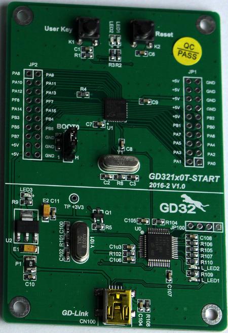
This article describes specifics for the GigaDevice GD321x0T-START evaluation board.

Preparing for J-Link
- Connect the J-Link to this pins:
| J-Link Pin | Connector | Pin | Name |
|---|---|---|---|
| VTref | JP1 | 20 | +5V |
| GND | JP1 | 19 | GND |
| TMS/SWDIO | JP2 | 6 | PA13 |
| TCK/SWCLK | JP2 | 9 | PA14 |
- Power the board via CN100.
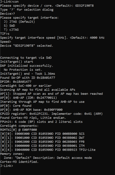
- Verify the Connection with e.g. J-Link Commander. The output should look as follows:
Example Project
The following example project was created with the SEGGER Embedded Studio project wizard and runs out-of-the-box on the GigaDevice GD321x0T-START.
It is a simple Hello World sample linked into the internal flash.
SETUP
- Embedded Studio: V8.10b
- Hardware: GigaDevice GD321x0T-START
- Link: File:GigaDevice GD32F190T8 TestProject ES V810b.zip
