Difference between revisions of "GD32330x"
(Created page with "This article describes specifics for the GD32330C-START evaluation board based on a GigaDevice GD32F330CB (Cortex-M4). File:GD32330C-START.jpg | 200px | thumb | right | GD32...") |
|||
| (6 intermediate revisions by the same user not shown) | |||
| Line 1: | Line 1: | ||
| − | This article describes specifics for the |
+ | This article describes specifics for the GigaDevice GD32330x Familiy. |
| − | [[File:GD32330C-START.jpg | 200px | thumb | right | GD322330C-START evaluation board]] |
||
__TOC__ |
__TOC__ |
||
| + | = GD32330C-START evaluation board = |
||
| − | = Using J-Link with GD32330C-START = |
||
| + | [[File:GD32330C-START.png | 200px | thumb | right | GD322330C-START evaluation board]] |
||
| + | The GD32330C-START evaluation board based is based on a GigaDevice GD32F330CB (Cortex-M4). |
||
| + | |||
| + | == Using J-Link with GD32330C-START == |
||
This section covers all necessary steps and requirements to establish a working connection with the J-Link to the GD32330C-START evaluation board. |
This section covers all necessary steps and requirements to establish a working connection with the J-Link to the GD32330C-START evaluation board. |
||
| − | == Minimum requirements == |
+ | === Minimum requirements === |
* Cortex-M4 is supported by all current J-Link models. In case of doubt, please check [[Software and Hardware Features Overview | Overview about which models / revisions support Cortex-M4]] |
* Cortex-M4 is supported by all current J-Link models. In case of doubt, please check [[Software and Hardware Features Overview | Overview about which models / revisions support Cortex-M4]] |
||
* J-Link software V6.72 or later |
* J-Link software V6.72 or later |
||
| − | == Preparing for J-Link == |
+ | === Preparing for J-Link === |
The GD32330C-START does not come with a standard debug connector but populates the debug SWD signals, Ground and VTReff on JP1 (4 pads), located on the left side of the MCU. Therefore, these pads have to be wired manually to connect J-Link to the evaluation board. |
The GD32330C-START does not come with a standard debug connector but populates the debug SWD signals, Ground and VTReff on JP1 (4 pads), located on the left side of the MCU. Therefore, these pads have to be wired manually to connect J-Link to the evaluation board. |
||
| − | === Connection Guide === |
+ | ==== Connection Guide ==== |
The following guide will describe how the GD32330C-START evaluation board can be connected to your J-Link Base V10 (or higher). Please note, that other J-Links might work as well but wiring might be slightly different. All needed information can be found in the probe related documentation. |
The following guide will describe how the GD32330C-START evaluation board can be connected to your J-Link Base V10 (or higher). Please note, that other J-Links might work as well but wiring might be slightly different. All needed information can be found in the probe related documentation. |
||
* Solder the pin headers to the pads listed in the table below, or simply solder pin headers to all pads on JP1. |
* Solder the pin headers to the pads listed in the table below, or simply solder pin headers to all pads on JP1. |
||
| Line 35: | Line 38: | ||
The result should be looking like this: |
The result should be looking like this: |
||
| − | [[File:GD32330C-START_wired.png | |
+ | [[File:GD32330C-START_wired.png | 150px | GD32330C-START wired with jumper cables]] |
* Power the board via the USB port (CN100). |
* Power the board via the USB port (CN100). |
||
| Line 42: | Line 45: | ||
[[File:GD32F330CB_Connect.PNG | 400px]] |
[[File:GD32F330CB_Connect.PNG | 400px]] |
||
| − | = Example projects = |
+ | == Example projects == |
The following, example projects were created with the [https://www.segger.com/products/development-tools/embedded-studio/ SEGGER Embedded Studio] project wizard and run out-of-the-box on the GD32330C-START evaluation board. |
The following, example projects were created with the [https://www.segger.com/products/development-tools/embedded-studio/ SEGGER Embedded Studio] project wizard and run out-of-the-box on the GD32330C-START evaluation board. |
||
| − | == Hello World == |
+ | === Hello World === |
The simple Hello World example project can be downloaded here: [[Media: GD32F330CB_Hello_World.zip | Hello World example project ]] |
The simple Hello World example project can be downloaded here: [[Media: GD32F330CB_Hello_World.zip | Hello World example project ]] |
||
| − | === Minimum requirements === |
+ | ==== Minimum requirements ==== |
* Embedded Studio Version 4.52 or later |
* Embedded Studio Version 4.52 or later |
||
* J-Link V10 or later |
* J-Link V10 or later |
||
Latest revision as of 17:19, 24 April 2020
This article describes specifics for the GigaDevice GD32330x Familiy.
Contents
GD32330C-START evaluation board
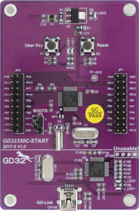
The GD32330C-START evaluation board based is based on a GigaDevice GD32F330CB (Cortex-M4).
Using J-Link with GD32330C-START
This section covers all necessary steps and requirements to establish a working connection with the J-Link to the GD32330C-START evaluation board.
Minimum requirements
- Cortex-M4 is supported by all current J-Link models. In case of doubt, please check Overview about which models / revisions support Cortex-M4
- J-Link software V6.72 or later
Preparing for J-Link
The GD32330C-START does not come with a standard debug connector but populates the debug SWD signals, Ground and VTReff on JP1 (4 pads), located on the left side of the MCU. Therefore, these pads have to be wired manually to connect J-Link to the evaluation board.
Connection Guide
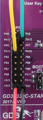
The following guide will describe how the GD32330C-START evaluation board can be connected to your J-Link Base V10 (or higher). Please note, that other J-Links might work as well but wiring might be slightly different. All needed information can be found in the probe related documentation.
- Solder the pin headers to the pads listed in the table below, or simply solder pin headers to all pads on JP1.
- Connect the board with e.g. jumper wires to your J-Link probe.
- The table below lists the pads that need to be connected to the J-Link.
- For information about the J-Link pinout please refer to the following page: J-Link SWD pinout.
| J-Link 20 pin debug interface | Pin on evaluation board |
|---|---|
| Pin 1 (VTref) | +3V3 |
| Pin 4 (GND) | GND |
| Pin 7 (SWDIO) | PA13 |
| Pin 9 (SWCLK) | PA14 |
The result should be looking like this:
- Power the board via the USB port (CN100).
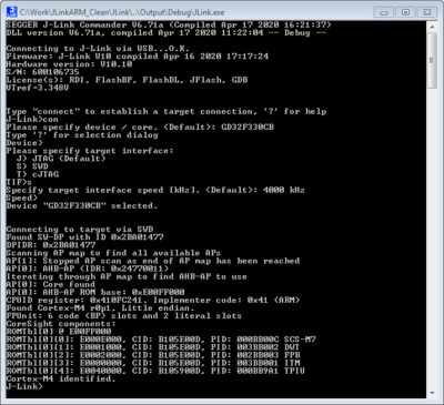
- Verify the Connection with e.g. J-Link Commander. The output should look as follows:
Example projects
The following, example projects were created with the SEGGER Embedded Studio project wizard and run out-of-the-box on the GD32330C-START evaluation board.
Hello World
The simple Hello World example project can be downloaded here: Hello World example project
Minimum requirements
- Embedded Studio Version 4.52 or later
- J-Link V10 or later


