GigaDevice GD32F310C-EVAL
Revision as of 18:21, 27 February 2024 by Joshua.Kozian (talk | contribs) (Created page with "__TOC__ This article describes specifics for the GigaDevice GD32F310C-EVAL evaluation board.<br> 450px == Preparing f...")
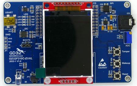
This article describes specifics for the GigaDevice GD32F310C-EVAL evaluation board.

Preparing for J-Link
- Connect the J-Link to this pins:
| J-Link Pin | Connector | Pin | Name |
|---|---|---|---|
| VTref | JP1 | 4 | +3V3 |
| GND | JP1 | 3 | GND |
| TMS/SWDIO | JP1 | 2 | IO |
| TCK/SWCLK | JP1 | 1 | CK |
- Power the board via CN100.
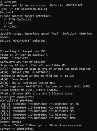
- Verify the Connection with e.g. J-Link Commander. The output should look as follows:
Example Project
The following example project was created with the SEGGER Embedded Studio project wizard and runs out-of-the-box on the GigaDevice GD32350C-START.
It is a simple Hello World sample linked into the internal flash.
SETUP
- Embedded Studio: V7.12a
- Hardware: GigaDevice GD32F310C-EVAL
- Link: File:GigaDevice GD32330CB TestProject ES V712a.zip
