Difference between revisions of "IndieSemi Realplum-EVK"
(→Preparing for J-Link) |
(→Preparing for J-Link) |
||
| (14 intermediate revisions by 2 users not shown) | |||
| Line 3: | Line 3: | ||
This article describes specifics for the IndieSemi Realplum EVK. |
This article describes specifics for the IndieSemi Realplum EVK. |
||
| + | [[File:IndieSemi_RealplumEVK.jpg|450px]] |
||
| − | TBD |
||
| − | [[File:NXP_JN5189-DK006.jpg|450px]] |
||
== Minimum requirements == |
== Minimum requirements == |
||
| − | *J-Link software V6. |
+ | *J-Link software V6.83d or later |
== Preparing for J-Link == |
== Preparing for J-Link == |
||
| + | The IndieSemi Realplum EVK does not come with a standard debug connector but populates the debug SWD signals on a 4 pin header (CON1). Therefore, it can be manually wired in case J-Link shall be connected to it. Apart from the debug signals, the board does not route Vdd (3.3V) to VTref by default which is required for the J-Link. The following guide will describe how the Realplum EVK can be connected to your J-Link Base V10 or higher. Other J-Links might work as well but wiring might be slightly different. All needed information can be found in the probe related documentation. |
||
| − | *Make sure that you install the correct "Upgrade Board" |
||
| − | *Connect the J-Link to the SWD header (P1) |
||
| − | *Power the board via external power supply / power jack (J4) |
||
| − | * Verify the Connection with e.g. [https://wiki.segger.com/J-Link_cannot_connect_to_the_CPU#Verify_functionality_using_J-Link_Commander J-Link Commander]. The output should look as follows: |
||
| + | * Solder a two pin header to J8 (VDD3V3) |
||
| + | * Close the soldered header using a jumper |
||
| + | * Now connect the board with e.g. jumperwires to your J-Link probe. |
||
| + | * The following table shows how the Signals should be connected on both the board and [https://www.segger.com/products/debug-probes/j-link/technology/interface-description/ J-Link] side. |
||
| + | |||
| + | {| class="wikitable" |
||
| + | |- |
||
| + | ! J-Link 20 pin debug interface !! Pin on eval board CON1 connector |
||
| + | |- |
||
| + | | Pin 1 (VTref) || Pin 1 (Vdd) |
||
| + | |- |
||
| + | | Pin 4 (GND) || Pin 4 (GND) |
||
| + | |- |
||
| + | | Pin 7 (SWDIO) || Pin 2 (SWD) |
||
| + | |- |
||
| + | | Pin 9 (SWCLK) || Pin 3 (SWC) |
||
| + | |- |
||
| + | |} |
||
| + | |||
| + | * Connect an external DC power supply to the board as follows: |
||
| + | **+3V DC to "J2 --> VDD3V3" |
||
| + | **GND DC to "J3 --> GND" |
||
| + | |||
| + | The resulting connection will then look like this:<br> |
||
| + | [[File:IndieSemi_RealplumEVK_connected.png|450px]] |
||
| + | * Verify the Connection with e.g. [https://wiki.segger.com/J-Link_cannot_connect_to_the_CPU#Verify_functionality_using_J-Link_Commander J-Link Commander]. The output should look as follows:<br> |
||
[[File:IndieSemi_Realplum_Connect.PNG|400px]] |
[[File:IndieSemi_Realplum_Connect.PNG|400px]] |
||
== Example Project== |
== Example Project== |
||
| − | The following example project was created with the SEGGER Embedded Studio project wizard and runs out-of-the-box on the IndieSemi Realplum. It is a simple Hello World sample linked into the internal flash. |
+ | The following example project was created with the SEGGER Embedded Studio project wizard and runs out-of-the-box on the IndieSemi Realplum. It is a simple Hello World sample linked into the internal flash.<br> |
'''SETUP''' |
'''SETUP''' |
||
*J-Link software: >= V6.83d |
*J-Link software: >= V6.83d |
||
Latest revision as of 16:42, 19 August 2020
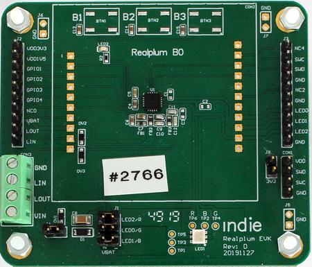
This article describes specifics for the IndieSemi Realplum EVK.
Minimum requirements
- J-Link software V6.83d or later
Preparing for J-Link
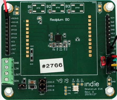
The IndieSemi Realplum EVK does not come with a standard debug connector but populates the debug SWD signals on a 4 pin header (CON1). Therefore, it can be manually wired in case J-Link shall be connected to it. Apart from the debug signals, the board does not route Vdd (3.3V) to VTref by default which is required for the J-Link. The following guide will describe how the Realplum EVK can be connected to your J-Link Base V10 or higher. Other J-Links might work as well but wiring might be slightly different. All needed information can be found in the probe related documentation.
- Solder a two pin header to J8 (VDD3V3)
- Close the soldered header using a jumper
- Now connect the board with e.g. jumperwires to your J-Link probe.
- The following table shows how the Signals should be connected on both the board and J-Link side.
| J-Link 20 pin debug interface | Pin on eval board CON1 connector |
|---|---|
| Pin 1 (VTref) | Pin 1 (Vdd) |
| Pin 4 (GND) | Pin 4 (GND) |
| Pin 7 (SWDIO) | Pin 2 (SWD) |
| Pin 9 (SWCLK) | Pin 3 (SWC) |
- Connect an external DC power supply to the board as follows:
- +3V DC to "J2 --> VDD3V3"
- GND DC to "J3 --> GND"
The resulting connection will then look like this:

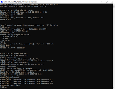
- Verify the Connection with e.g. J-Link Commander. The output should look as follows:
Example Project
The following example project was created with the SEGGER Embedded Studio project wizard and runs out-of-the-box on the IndieSemi Realplum. It is a simple Hello World sample linked into the internal flash.
SETUP
- J-Link software: >= V6.83d
- Embedded Studio: >= V4.52b
- Hardware: IndieSemi Realplum EVK
- Link: File:IndieSemi Realplum TestProject ES V452b.zip

