Difference between revisions of "NXP FRDM-MCXA156"
(→Preparing for J-Link) |
|||
| Line 5: | Line 5: | ||
== Preparing for J-Link == |
== Preparing for J-Link == |
||
| − | *Connect the J-Link to |
+ | *Connect the J-Link to J24, JP8 hast to set in order to disable MCU-Link on the PCB and work with J-Link. |
| − | *Power the board via USB |
+ | *Power the board via USB J21. |
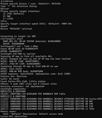
* Verify the Connection with e.g. [https://wiki.segger.com/J-Link_cannot_connect_to_the_CPU#Verify_functionality_using_J-Link_Commander J-Link Commander]. The output should look as follows: |
* Verify the Connection with e.g. [https://wiki.segger.com/J-Link_cannot_connect_to_the_CPU#Verify_functionality_using_J-Link_Commander J-Link Commander]. The output should look as follows: |
||
[[File:NXP_FRDM-MCXA156_MCXA156VL_connect.png|400px]] |
[[File:NXP_FRDM-MCXA156_MCXA156VL_connect.png|400px]] |
||
Revision as of 11:06, 13 March 2024
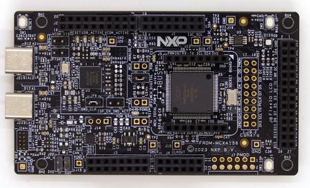
This article describes specifics for the NXP FRDM-MCXA156 evaluation board.

Preparing for J-Link
- Connect the J-Link to J24, JP8 hast to set in order to disable MCU-Link on the PCB and work with J-Link.
- Power the board via USB J21.
- Verify the Connection with e.g. J-Link Commander. The output should look as follows:
Example Project
The following example project was created with the SEGGER Embedded Studio project wizard and runs out-of-the-box on the NXP FRDM-MCXA156.
It is a simple Hello World sample linked into the internal flash.
SETUP
- J-Link software: V7.96c
- Embedded Studio: V7.20
- Hardware: NXP FRDM-MCXA156
- Link: File:NXP X-FRDM-MCXA156 MCXA156 TestProject ES 7V20.zip
