Difference between revisions of "NXP MIMXRT1060-EVKC"
| Line 15: | Line 15: | ||
** Note: By default, the hardware supports SWD only. JTAG must be explicitly enabled by following steps described in the board user manual by NXP. |
** Note: By default, the hardware supports SWD only. JTAG must be explicitly enabled by following steps described in the board user manual by NXP. |
||
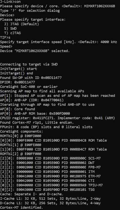
* Verify the Connection with e.g. [https://wiki.segger.com/J-Link_cannot_connect_to_the_CPU#Verify_functionality_using_J-Link_Commander J-Link Commander]. The output should look as follows: |
* Verify the Connection with e.g. [https://wiki.segger.com/J-Link_cannot_connect_to_the_CPU#Verify_functionality_using_J-Link_Commander J-Link Commander]. The output should look as follows: |
||
| − | [[File: |
+ | [[File:NXP_MIMXRT1062DVL6B_connect.png|400px]] |
== Example Project == |
== Example Project == |
||
Revision as of 13:26, 12 December 2022
This article describes specifics for the NXP MIMXRT1060-EVKC evaluation board. It can be used to test & verify NXP i.MXRT1060 support.
Minimum requirements
- J-Link software V7.82a or later
Preparing for J-Link
- Power the board via Micro-USB or power jack (5V, center-positive).
- Note: When powering the hardware via power jack, pins 1 and 2 on jumper J40 must be closed.
- Note: When powering the hardware via Micro-USB OTG J48, pins 3 and 4 on jumper J40 must be closed.
- Connect the hardware to J-Link using a 20pin ribbon cable for J2
- Note: By default, the hardware supports SWD only. JTAG must be explicitly enabled by following steps described in the board user manual by NXP.
- Verify the Connection with e.g. J-Link Commander. The output should look as follows:
Example Project
The following example project was created with the SEGGER Embedded Studio project wizard and runs out-of-the-box on the NXP MIMXRT1060-EVKC. The board must be configured to boot from the internal QSPI flash:
| SW2 switches | |||
|---|---|---|---|
| 1 | 2 | 3 | 4 |
| OFF | OFF | OFF | OFF |
| SW4 switches | |||
|---|---|---|---|
| 1 | 2 | 3 | 4 |
| OFF | OFF | ON | OFF |
More information on the different boot modes and how to configure them can be found in the board user manual by NXP.
The sample project is a simple Cnt++ loop linked into the internal (Q)SPI flash.
SETUP
- J-Link software: V7.82a
- Embedded Studio for ARM: V6.40
- Hardware: NXP MIMXRT1060-EVK
- Link: File:MIMXRT1060-EVK QSPI.zip
