Difference between revisions of "NXP PNEV76FAMA"
(→Preparing for J-Link) |
(→Preparing for J-Link) |
||
| Line 11: | Line 11: | ||
*For board REV D remove jumper J20 3-4 and connect pin 4 of J20 to any ground e.g. TP4. Keep J25 open. |
*For board REV D remove jumper J20 3-4 and connect pin 4 of J20 to any ground e.g. TP4. Keep J25 open. |
||
*Connect the J-Link to the debug connector (J21) |
*Connect the J-Link to the debug connector (J21) |
||
| − | *Power the board via |
+ | *Power the board via USB (J5) |
Afterwards, the board should look similar to this:<br> |
Afterwards, the board should look similar to this:<br> |
||
Revision as of 13:36, 28 April 2022
This article describes specifics for the NXP PNEV76FAMA evaluation board. It can be used to test & verify PN76 device support with J-Link.
Minimum requirements
- J-Link software V7.65b or later
Preparing for J-Link
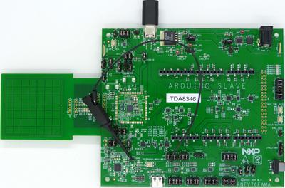
- For board REV D remove jumper J20 3-4 and connect pin 4 of J20 to any ground e.g. TP4. Keep J25 open.
- Connect the J-Link to the debug connector (J21)
- Power the board via USB (J5)
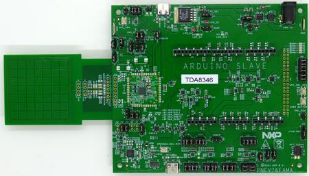
Afterwards, the board should look similar to this:

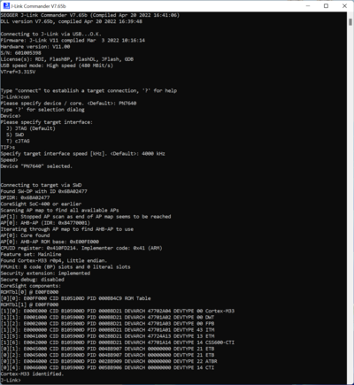
Verify the Connection with e.g. J-Link Commander. The output should look as follows:
Example Project
The following example project was created with the SEGGER Embedded Studio project wizard and runs out-of-the-box on the NXP S32K3X4EVB. It is a simple Hello World sample linked into the internal flash.
SETUP
- J-Link software: V7.65b
- Embedded Studio: V6.22
- Hardware: NXP PNEV76FAMA
- Link: File:NXP PNEV76FAMA ES V622.zip

