Difference between revisions of "Pimoroni Tiny 2040"
(Created page with " thumb | right | 500 px | Pimoroni Tiny 2040 (RP2040) The Pimoroni Tiny 2040 is a Raspberry Pi RP2040 evaluation board. As the name sugges...") |
|||
| Line 1: | Line 1: | ||
| − | [[File: |
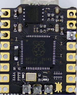
+ | [[File: Pimoroni_Tiny2040_front.JPG | thumb | right | 300 px | Pimoroni Tiny 2040 (RP2040)]] |
The Pimoroni Tiny 2040 is a [[Raspberry Pi RP2040]] evaluation board. |
The Pimoroni Tiny 2040 is a [[Raspberry Pi RP2040]] evaluation board. |
||
As the name suggests, it is particularly small (~ 22.9 x 18.2 x 6mm (L x W x H, including the USB-C port)). |
As the name suggests, it is particularly small (~ 22.9 x 18.2 x 6mm (L x W x H, including the USB-C port)). |
||
| Line 14: | Line 14: | ||
== Setting up with J-Link == |
== Setting up with J-Link == |
||
| − | [[File: Pimoroni_Tiny2040_back.JPG | thumb | right | |
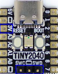
+ | [[File: Pimoroni_Tiny2040_back.JPG | thumb | right | 200 px | Debug interface connection]] |
The Pimoroni Tiny 2040 evaluation board comes with an external SWD debug connector (3 pins: SWCLK, GND, SWDIO). |
The Pimoroni Tiny 2040 evaluation board comes with an external SWD debug connector (3 pins: SWCLK, GND, SWDIO). |
||
To set the board up with J-Link, the following steps are required: |
To set the board up with J-Link, the following steps are required: |
||
Revision as of 16:27, 23 April 2021
The Pimoroni Tiny 2040 is a Raspberry Pi RP2040 evaluation board. As the name suggests, it is particularly small (~ 22.9 x 18.2 x 6mm (L x W x H, including the USB-C port)).
Features (selection)
- RP2040 MCU
- 8MB on board QSPI flash
- USB-C
- On board RGB-LED
- 12 I/O pins
- external debug connector pads
For further information please refer to the Pimoroni Tiny 2040 web page.
Setting up with J-Link
The Pimoroni Tiny 2040 evaluation board comes with an external SWD debug connector (3 pins: SWCLK, GND, SWDIO). To set the board up with J-Link, the following steps are required:
- Solder a 3-pin pin strip to the debug connector pads.
-
Solder a pin Strip to the GPIO pads of the evaluation board. The relevant pad is Pad 3 3V3 (3V)
-
Connect the J-Link to the evaluation board, using jumper wires as follows:
Pin Tiny 2040 Pin J-Link Signal "DEBUG" "SWC" 9 SWCLK "DEBUG" " - " 4 GND "DEBUG" "SWD" 7 SWDIO "3V" Pad 3 1 VTref
Note: For a more reliable, simpler solution, the SEGGER Flying Wire Adapter is recommended.
Example Projects
To run the following example projects the following prerequisites need to be met:
- J-Link software V7.00b or later
- J-Link HW revision 11 or later (J-Link Edu Mini and J-Trace Pro V1 or later also supported)
- SEGGER Embedded Studio V5.42a or later

