Difference between revisions of "ST NUCLEO-F030R8"
(Created page with "__TOC__ This article describes specifics for the ST NUCLEO-F030R8 evaluation board.<br> 450px == Preparing for J-Link == *Connect the J-Link to...") |
(→Preparing for J-Link) |
||
| Line 5: | Line 5: | ||
== Preparing for J-Link == |
== Preparing for J-Link == |
||
| + | |||
| − | *Connect the J-Link to ...... |
||
| + | * Connect the board with jumping wires to your J-Link (see table below)<br>For information about the J-Link pinout please refer to the following page: [https://www.segger.com/products/debug-probes/j-link/technology/interface-description/#swd-connector-pinout J-Link SWD pinout]. |
||
| − | *Power the board via........ |
||
| + | |||
| + | {| class="wikitable" |
||
| + | |- |
||
| + | ! J-Link 20 pin debug interface !! Pin on evaluation board |
||
| + | |- |
||
| + | | Pin 1 (VTref, red) || Pin 16 at CN7 pin header |
||
| + | |- |
||
| + | | Pin 4 (GND, black) || Pin 8 at CN7 pin header |
||
| + | |- |
||
| + | | Pin 7 (SWDIO, green) || Pin 4 at CN4 pin header |
||
| + | |- |
||
| + | | Pin 9 (SWCLK, yellow) || Pin 2 at CN4 pin header |
||
| + | |- |
||
| + | | Pin 15 (RESET, blue) || Pin 5 at CN4 pin header |
||
| + | |} |
||
| + | The result should be looking like this: |
||
| + | |||
| + | [[File:ST_NUCLEO-F030R8_wired.jpg | 500px | ST NUCLEO-F030R8 wired with jumper cables]] |
||
| + | |||
| + | *Power the board via CN1 (Mini USB) |
||
* Verify the Connection with e.g. [https://wiki.segger.com/J-Link_cannot_connect_to_the_CPU#Verify_functionality_using_J-Link_Commander J-Link Commander]. The output should look as follows: |
* Verify the Connection with e.g. [https://wiki.segger.com/J-Link_cannot_connect_to_the_CPU#Verify_functionality_using_J-Link_Commander J-Link Commander]. The output should look as follows: |
||
[[File:ST_STM32F030R8_CONNECT.PNG|400px]] |
[[File:ST_STM32F030R8_CONNECT.PNG|400px]] |
||
Revision as of 16:37, 3 August 2023
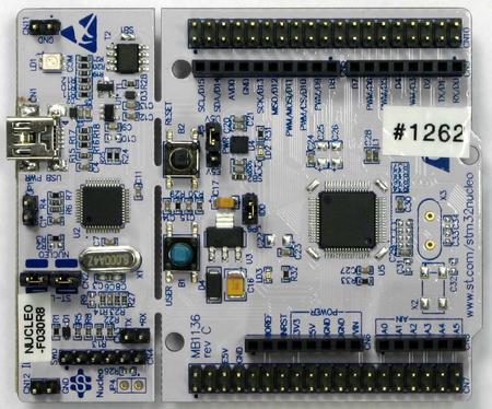
This article describes specifics for the ST NUCLEO-F030R8 evaluation board.

Preparing for J-Link
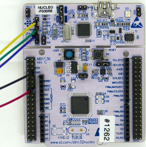
- Connect the board with jumping wires to your J-Link (see table below)
For information about the J-Link pinout please refer to the following page: J-Link SWD pinout.
| J-Link 20 pin debug interface | Pin on evaluation board |
|---|---|
| Pin 1 (VTref, red) | Pin 16 at CN7 pin header |
| Pin 4 (GND, black) | Pin 8 at CN7 pin header |
| Pin 7 (SWDIO, green) | Pin 4 at CN4 pin header |
| Pin 9 (SWCLK, yellow) | Pin 2 at CN4 pin header |
| Pin 15 (RESET, blue) | Pin 5 at CN4 pin header |
The result should be looking like this:
- Power the board via CN1 (Mini USB)
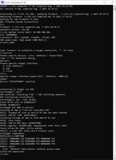
- Verify the Connection with e.g. J-Link Commander. The output should look as follows:
Example Project
The following example project was created with the SEGGER Embedded Studio project wizard and runs out-of-the-box on the ST NUCLEO-F030R8.
It is a simple Hello World sample linked into the internal flash.
SETUP
- J-Link software: V7.90
- Embedded Studio: V7.20
- Hardware: ST NUCLEO-F030R8
- Link: File:ST STM32F030R8 TestProject ES V720.zip

