Difference between revisions of "Renesas ASSP EASY"
(→Internal Flash) |
|||
| Line 8: | Line 8: | ||
! Flash Bank || Base address !! Size || J-Link Support |
! Flash Bank || Base address !! Size || J-Link Support |
||
|- |
|- |
||
| − | | |
+ | | Code Flash || 0x00000000 || 128 KB || style="text-align:center;"| {{YES}} |
| + | |- |
||
| + | | Config Flash || 0x00000000 || 44 B || style="text-align:center;"| {{YES}} |
||
| + | |- |
||
| + | | Data Flash || 0x00000000 || 4 KB || style="text-align:center;"| {{YES}} |
||
| + | |||
|} |
|} |
||
Revision as of 16:10, 18 March 2024
The Renesas ASSP easy are [SHORT_DESCRIPTION]
Contents
Flash Banks
Internal Flash
| Flash Bank | Base address | Size | J-Link Support |
|---|---|---|---|
| Code Flash | 0x00000000 | 128 KB | |
| Config Flash | 0x00000000 | 44 B | |
| Data Flash | 0x00000000 | 4 KB |
ECC Flash [OPTIONAL]
- Describe ECC Flash restriction here.
QSPI Flash
QSPI flash programming requires special handling compared to internal flash. For more information about this, please see the QSPI Flash Programming Support article.
J-Link supports multiple pin configurations for [DEVICE]. The default loader is marked in bold.
| Device | Base address | Maximum size | Supported pin configuration |
|---|---|---|---|
| [DEVICE] | [BANK_BASE_ADDRESS] | [MAX_SPI_FLASH_SIZE] MB |
|
ECC RAM [OPTIONAL]
- Describe ECC RAM restriction here.
Vector Table Remap [OPTIONAL]
- Describe Vector Table Remap here..
Watchdog Handling
- The device does not have a watchdog.
- The device has a watchdog [WATCHDOGNAME].
- The watchdog is fed during flash programming.
- If the watchdog is enabled, it is turned off during flash programming and turned back on afterwards.
Multi-Core Support [OPTIONAL]
Before proceeding with this article, please check out the generic article regarding Multi-Core debugging here.
The [DeviceFamily]family comes with a variety of multi-core options.
Some devices from this family feature a secondary core which is disabled after reset / by default.
Some of the are available with enabled lockstep mode, only.
In below, the debug related multi-core behavior of the J-Link is described for each core:
Main core
Init/Setup
- Initializes the ECC RAM, see XXX
- Enables debugging
Reset
- Device specific reset is performed, see XXX
Attach
- Attach is not supported because the J-Link initializes certain RAM regions by default
Secondary core(s)
Init/Setup
- If the main core session has not been started / debugging is not enabled yet, the secondary core executes the enable debug sequence.
- If the secondary core is not enabled yet, it will be enabled / release from reset
Reset
No reset is performed.
Attach
- Attach is supported / desired
Device Specific Handling
Connect
Reset
- The device uses normal Cortex-M reset, no special handling necessary, like described here.
- The device uses Cortex-M Core reset, no special handling necessary, like described here.
- The device uses Cortex-M Rest Pin, no special handling necessary, like described here.
- The device uses Cortex-A reset, no special handling necessary, like described here.
- The device uses Cortex-R reset, no special handling necessary, like described here.
- The device uses ARMv8-A reset, no special handling necessary, like described here.
- The device uses ARMv8-R reset, no special handling necessary, like described here.
- The device uses custom reset:.....
Limitations
Dual Core Support
Some XXX devices feature a second core. Right now, the J-Link software does support the main core, only. Support for the second core is planned for future versions.
Attach
Attach is not supported by default because the J-Link initializes certain RAM regions by default.
Security
Evaluation Boards
Example Application
Tracing on [SiliconVendor] [DeviceFamily]
This section describes how to get started with trace on the [SiliconVendor] [DeviceFamily] MCUs. This section assumes that there is already a basic knowledge about trace in general (what is trace, what different implementations of trace are there, etc.). If this is not the case, we recommend to read Trace chapter in the J-Link User Manual (UM08001).
- The sample projects come with a pre-configured project file for Ozone that runs out-of-the box.
- The following sample project is designed to be used with J-Trace PRO for streaming trace, J-Link Plus for buffer tracing (TMC/ETB trace) and Ozone to demonstrate streaming trace.
- In order to rebuild the sample project, SEGGER Embedded Studio can be used.
- The examples are shipped with a compiled .JLinkScriptfile, should you need the original source, please get in touch with SEGGER directly via our support system: https://www.segger.com/ticket/.
- To create your own .JLinkScriptfile you can use the following guide as reference: How_to_configure_JLinkScript_files_to_enable_tracing
Tracing on [SiliconVendor] [DeviceName] ([Boardname]-optional)
Minimum requirements
In order to use trace on the [SiliconVendor] [DeviceName] MCU devices, the following minimum requirements have to be met:
- J-Link software version Vx.xxx or later
- Ozone Vx.xxx or later (if streaming trace and / or the sample project from below shall be used)
- J-Trace PRO for Cortex-M HW version V3.0 or later for streaming trace
- J-Link Plus V12 or later for TMC/ETB trace
To rebuild the project our IDE Embedded Studio can be used. The recommended version to rebuild the projects is V6.30. But the examples are all prebuild and work out-of-the box with Ozone, so rebuilding is not necessary.
Streaming trace
The project below has been tested with the minimum requirements mentioned above and a [Boardname].
- Example project: ST_STM32H7_Trace_Tutorial_Project.zip
Trace buffer (TMC/ETB)
The project below is utilizing the on-chip trace buffer (it is not meant for streaming trace).
- Example Project: ST_STM32H7_TraceBuffer_Tutorial_Project.zip
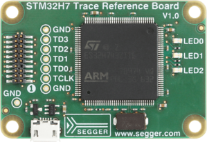
Tested Hardware
Reference trace signal quality
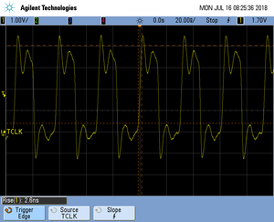
The following pictures show oscilloscope measurements of trace signals output by the "Tested Hardware" using the example project. All measurements have been performed using a Agilent InfiniiVision DSO7034B 350 MHz 2GSa/s oscilloscope and 1156A 1.5 GHz Active Probes. If your trace signals look similar on your trace hardware, chances are good that tracing will work out-of-the-box using the example project. More information about correct trace timing can be found at the following website.
Trace clock signal quality
The trace clock signal quality shows multiple trace clock cycles on the tested hardware as reference.
Rise time
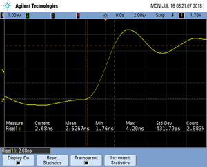
The rise time of a signal shows the time needed for a signal to rise from logical 0 to logical 1. For this the values at 10% and 90% of the expected voltage level get used as markers. The following picture shows such a measurement for the trace clock signal.
Setup time
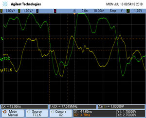
The setup time shows the relative setup time between a trace data signal and trace clock. The measurement markers are set at 50% of the expected voltage level respectively. The following picture shows such a measurement for the trace data signal 0 relative to the trace clock signal.


